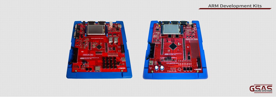
GSAS LPC 1768

The GSAS LPC 1768 is a development and evaluation board that is built on the NXP LPC1768 platform, an ARM Cortex-M3 based microcontroller for embedded applications featuring system enhancements such as enhanced debug features and a higher level of support block integration. With its extensive features and capabilities, it is a board that can accelerate your development with ARM-based products. This board also serves as an excellent educational tool for training of next-generation embedded engineers at educational establishments.

  • Powered by PC’s USB port.
  • Communicates with host PC through its on-board serial port – Rs 232C/USB Port  which is provided for In-System-Programming
  • On-chip 512K bytes Flash, 64k Bytes RAM are available to user
  • Provision for USB Plug in device interface
  • Two on-chip UART ports are terminated on 9 pin D type (Female) connectors J1 and J2
  • Provision for CAN interface (CAN0 and CAN1 are terminated on two 9 Pin D type (male) connectors J5 and J6
  • USB interface uses the standard USB connector for the full speed USB 2.0 peripheral of LPC 1768 device
  • SD memory card connector that supports a wide range of memory cards
  • The status of the port lines can be monitored through on board 8 LED’s
  • Color QVGA TFT LCD with touch screen is available for the user interface
  • On board RESET switch and INT switch
  • Provision for onboard keyboard connector and speaker
  • On-chip 2 analog voltage controllers for ADC input
  • The prototyping area provides pads for connecting ports
  • Flexible configuration using jumpers
  • On-chip I2C and SPI interfaces are available to user
  • Provision for on board Ethernet connector
  • GSAS LPC 1768 Provides two 8 digit 7 segment displays and 4×4 matrix Hex keypad
  • On-board JTAG connector is provided for connecting JTAG based debuggers
  • On Board 20 pin JTAG connector for debugging/programming various applications
  • On board power supply connector and 26 pin FRC connector are available for interfacing the GSAS LPC 1768 board to some of the GSAS Interface Modules such as Seven Segment Display, Elevator, Traffic Lights, Dual DAC, Txdr ADCetc.,
  • MCU : NXP LPC 1768
  • MCU clock : 100 Mhz
  • On-chip RAM : 64KB
  • On-chip Flash : 512KB
  • Serial Ports : 2(On-chip)
  • CAN Ports : 2(On-chip)
  • USB Interface : 1(On-chip)
  • PCB Size : 170 X 202 mm
  • JTAG Interface : 20 Pin standard connector
  • Power connector : Standard USB connector
  • LPC 1768 Evaluation board
  • USB Cable
  • Driver software CD
  • User manual
  • Debugger
  • GSAS ADP DC5
  • GSAS PS M2 5V@ 3A; ±12V @250mA; +30V@100mA
  • Standard Pentium PC with USB port & CD
  • Windows 2000/XP/Vista OS.
  • 300MB of Hard disk space.
  • 512MB of RAM.

GSAS LPC 2929

The GSAS LPC 2929 board is built around the NXP LPC 2929, an ARM9 processor-based device, allowing you to create and test working programs for this advanced architecture. This board has a wide range of interfaces making it a great starting point for your next ARM project.

  • This board hosts the LPC2929 microcontroller from NXP with an embedded ARM968E-S processor core and JTAG interface. In addition, the driver chips for the external communication interfaces are included.
  • All microcontroller IO port pins are accessible via connectors.
  • The device drivers can be disabled via jumpers to have control of the microcontroller I/O pins.
  • The board is powered by a USB port.
  • A serial connection is provided for In-System-Programming (RS-232).
  • There is a provision for CAN and USB interfaces enabling industrial automation as well as automotive applications.
    The board has 8 LEDs, analog input (via potentiometer) and three switches as GPIO.
  • The onboard JTAG connector is provided for connecting JTAG based debuggers like KEIL ULINK, SEGGER J-LINK, etc.,
    This board, with a power supply connector and 26 pin FRC connector can be interfaced with interface modules such as Seven Segment Display, Elevator, Traffic Lights, Dual DAC, Txdr ADC etc… which are developed by GSASMSPL.
    With its extensive features and capabilities, it is a board that can accelerate your development with ARM-based products.
  • This board also serves as an excellent educational tool for training of next-generation embedded engineers at educational establishments.
  • MCU :NXP LPC 2929
  • MCU clock :125 Mhz
  • On-chip RAM :56KB
  • On-chip Flash :768KB
  • Serial Ports :1(On-chip)
  • CAN Ports :2(On-chip)
  • USB Interface :1(On-chip)
  • PCB Size :170 X 202 mm
  • JTAG Interface :20 Pin standard IDC connector
  • Power connector :Standard USB Type -B connector
  • LPC 2929 Evaluation board
  • USB Cable
  • Driver software CD
  • User manual
  • Debugger
  • GSAS PS M2 5V@3A; ±12V @250mA;+30V@100mA (Required for some of the interface modules)
  • Standard Pentium PC with USB port
  • CD ROM Drive
  • Windows 2000/XP/Vista OS
  • 300MB of Hard disk space
  • 512MB of RAM

Keil MCB 1800

The Keil MCB1800 Evaluation Boards enable you to create and test working programs based on the NXP LPC1850 family of ARM Cortex™-M3 processor-based devices.

The MCB1800 Evaluation Board is available in two different configurations:

  • The MCB1850 Evaluation Board is populated with an NXP LPC1850 device
  • The MCB1857 Evaluation Board is populated with a NXP LPC1857 device
  • 180MHz ARM Cortex-M3 processor-based MCU in LBGA256
  • On-Chip SRAM: 136KB (LPC1857), 200KB (LPC1850)
  • On-Chip Flash: 1MB dual bank (LPC1857), no on-chip Flash (LPC1850)
  • On-Board Memory: 16MB NOR Flash, 4MB Quad-SPI Flash, 16 MB SDRAM, & 16KB
    EEPROM (I2C)
  • Color QVGA TFT LCD with touchscreen
  • 10/100 Ethernet Port
  • High-speed USB 2.0 Host/Device/OTG interface (USB host + Micro USB Device/OTG
    connectors)
  • Full-speed USB 2.0 Host/Device interface (USB host + micro USB Device connectors)
  • CAN interfaces
  • Serial/UART Port
  • MicroSD Card Interface
  • 4 user push-buttons + reset
  • Digital Temperature Sensor (I2C)
  • Analog Voltage Control for ACD Input
  • Audio CODEC with Line-In/Out and Microphone/headphone connector + Speaker
  • Debug Interface Connectors
  • 20-pin JTAG (0.1 inch)
  • 10-pin Cortex debug (0.05 inch)
  • 20-pin Cortex debug + ETM Trace (0.05 inch)

Arm MPS2+ FPGA Prototyping Board

The Arm MPS2+ FPGA Prototyping Board, is an affordable development board. The platform offers a relatively large FPGA for prototyping Cortex-M based designs with a range of debug options. It also includes useful peripherals such as: PSRAM, Ethernet, touch screen, Audio, VGA, SPI and GPIO. The MPS2+ is supplied with fixed encrypted FPGA implementations of all the Cortex-M processors. The platform supports online software development using mbed
for the full Cortex-M family. It allows:

  • Rapid FPGA prototyping for Cortex-M with example designs and software support
  • Low cost feature rich FPGA development platform supporting the entire Cortex-M processor range
  •  180MHz ARM Cortex-M3 processor-based MCU in LBGA256
  • On-Chip SRAM: 136KB (LPC1857), 200KB (LPC1850)
  • On-Chip Flash: 1MB dual bank (LPC1857), no on-chip Flash (LPC1850)
  • On-Board Memory: 16MB NOR Flash, 4MB Quad-SPI Flash, 16 MB SDRAM, & 16KB
    EEPROM (I2C)
  • Color QVGA TFT LCD with touchscreen
  • 10/100 Ethernet Port
  • High-speed USB 2.0 Host/Device/OTG interface (USB host + Micro USB Device/OTG
    connectors)
  • Full-speed USB 2.0 Host/Device interface (USB host + micro USB Device connectors)
  • CAN interfaces
  • Serial/UART Port
  • MicroSD Card Interface
  • 4 user push-buttons + reset
  • Digital Temperature Sensor (I2C)
  • Analog Voltage Control for ACD Input
  • Audio CODEC with Line-In/Out and Microphone/headphone connector + Speaker
  • Debug Interface Connectors
  • 20-pin JTAG (0.1 inch)
  • 10-pin Cortex debug (0.05 inch)
  • 20-pin Cortex debug + ETM Trace (0.05 inch)

Arm MPS3 FPGA Prototyping Board

The Arm MPS3 FPGA Prototyping Board is an FPGA prototyping platform, which allows designers to design systems easily. The board features a large FPGA to implement complex embedded designs (even including small Cortex-A class cores) and many expansion connectors to plug in other systems. Key benefits of the MPS3 board include:

  • FPGA capacity 5x larger than MPS2+
  • A wide range of connectors and peripherals
  • Prototype Linux applications
FPGA Xilinx Kintex Ultrascale KU115 FPGA, 1,451k logic cells
Support for encrypted FPGA images and Partial Reconfiguration
 Memory 8MB BRAM
4GB DDR4 SODIMM (by default, upgradeable to 8GB)
16GB eMMC
8MB QSPI Flash
 Debug JTAG
10-pin Cortex debug connector
20-pin Cortex debug and ETM connector
16-bit Trace Mictor connector
ILA for ChipScope ProTM / IdentifyTM
CMSIS-DAP support
Board peripherals USB2.0 Dual port Host Controller
10/100Mb Ethernet Controller
uSD-Card slot
Audio (line in/out and mic)
QSVA Colour Display & Touch Screen – 8-bit parallel interface
HDMI 1.2 PHY
Four Virtual UARTs over USB CONFIG PORT
Eight user LEDs/switches
Two user push buttons
Real time clock
Six programmable clocks
Expansion Two Arduino Expansion connectors
Four PMOD connectors
FMC-HPC connector – Up to 160 I/Os
Form factor 170x170mm mini ITX

Contact Us

Bengaluru (Headquarters)

Chennai

tn@gsasmspl.com

+91 98450 19071

Delhi

delhi@gsasmspl.com

+91 98450 55228

Hyderabad

ts@gsasmspl.com

+91 98450 19029

+91 98450 19013

Mumbai

mh@gsasmspl.com

+91 98450 42976

+91 98450 19013

Pune

mh@gsasmspl.com

+91 98450 42976

+91 98450 19013

Vizag

vizag@gsasmspl.com

+91 98450 98535

+91 98450 42981