What most people don’t seem to grasp is that every aspect of the PCB is critical. It all plays a significant part in the operation of the final product. The layer stack is no different. We need to keep in mind materials and the intricacies therein, including thickness, weave, dielectric constants, and more.
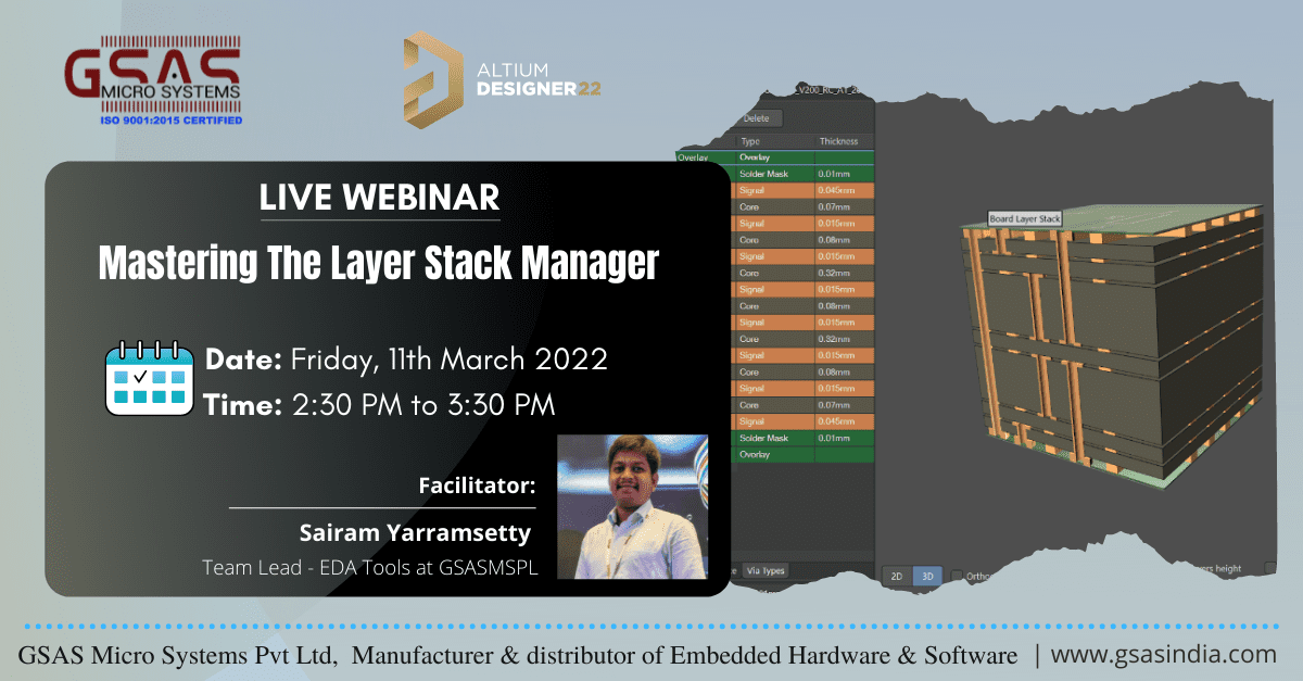
A proper layer stack is needed for each and every design, so it’s important to know how to navigate the layer stack manager and all of its features. By mastering the layer stack manager you can quickly create a new stackup from existing templates, swap out approved materials with the materials library, and more. Join us for this webinar to learn how you can take control of your stackup.
Join our webinar to learn how you can:
- Materials Library
- Layer Stack Templates & Presets
- Via types
- Back drilling
- Impedance profiles


