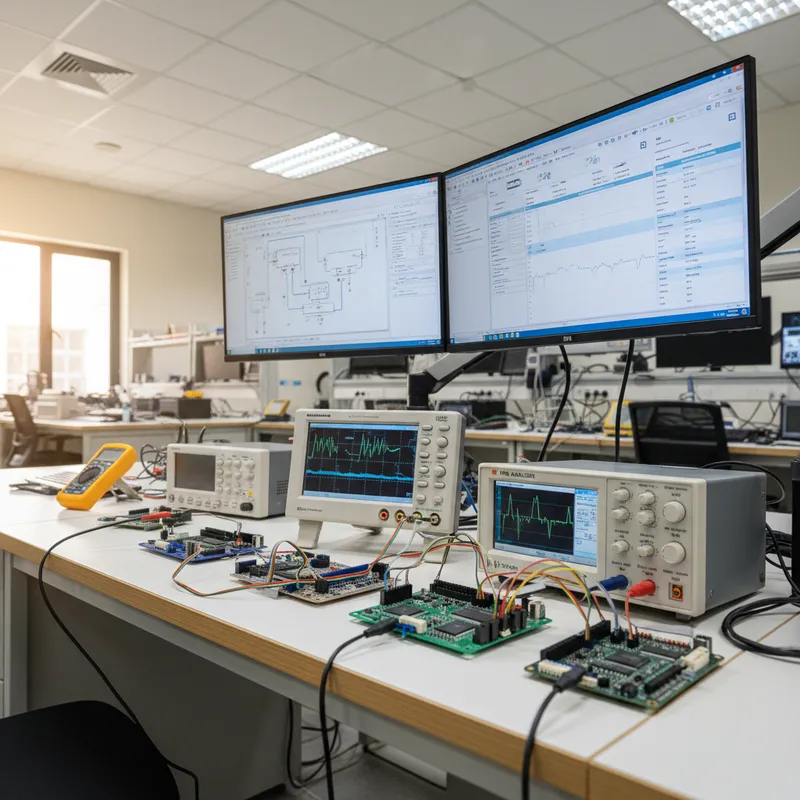
With modern digital designs featuring high-speed circuitry, multiple devices, densely populated boards, and multiple supply rails, the demands placed on a design’s DC power distribution network warrants a more analytical approach to its design. The DC analysis of a Power Delivery Network (PDN), or the results of its DC Power Integrity (PI-DC), is basically aimed at ensuring that adequate copper has been provided in the path from the voltage sources to the loads – in other words, that the planes, traces, and vias on the board are of sufficient size (and characteristics) to meet the power consumption requirements of the devices on the board.
What PDN Analyzer Does
PDN Analyzer is Altium Designer’s PI-DC (Power Integrity, Direct Current) simulation tool. Rather than treating power and ground as ideal nets, it solves the actual DC behaviour of the copper geometry on your PCB, the planes, polygons, traces, and vias that carry current from regulators to loads, and reports two physically meaningful results: voltage drop (IR drop) at every load pin, and current density across every shape on every layer (Altium Designer Documentation, PDN Analyzer).
The IR drop problem is straightforward in principle: the resistance embodied in the board’s power supply shapes (traces, polygons, planes) consumes power and voltage, robbing those from the loads. PDN Analyzer extracts that resistance directly from the live PCB design, no external data import or netlist regeneration, and shows where copper is too thin, too narrow, or too far from where current actually wants to flow.
A note on licensing for Indian design teams evaluating the tool: PDN Analyzer is not bundled into a base Altium Designer seat. It is an installable software extension and requires a separate, valid PDN Analyzer subscription. Newer Altium Designer releases ship a successor extension, Power Analyzer by Keysight, which is also an optional add-on with a 14-day trial available to all subscription tiers (Altium, Power Analyzer by Keysight). Both run inside the PCB editor and read the active design without manual export.
Common Findings on Indian PCB Designs
The categories of issues PDN Analyzer surfaces are well-known to anyone who has done DC sign-off on a dense, multi-rail board:
- Undersized power planes split into too many islands by signal escape routes, leaving narrow copper bridges that quietly become the dominant resistance in a low-voltage rail.
- Neckdown traces under high-current pads: typically where a 1.0 V or 1.2 V core rail enters a BGA or QFN through a constrained breakout, pushing local current density well past the copper’s safe ampacity for the chosen weight and temperature rise.
- Missing or under-stitched return paths near switching regulators, where buck converter input and output loops route through too few ground vias, raising effective return-path resistance and pulling reference voltage at downstream loads.
- Voltage drop through narrow GND traces returning to MOSFET source pins in motor-drive and load-switch sections, where the return path is silently routed as a trace rather than a plane, causing the regulator’s sense point to disagree with the actual load voltage.
These are categories of problems, not specific customer narratives, but they are the recurring failure modes PDN Analyzer is built to expose before fabrication, not after a board is on the bench with a thermal camera.
When to Run PDN Analyzer
Altium positions the tool across three stages of the PCB design flow (Altium Designer Documentation, PDN Analyzer):
- Pre-layout (planning): rough-size copper, plane stack-up, and regulator placement before routing begins. Cheap to change here.
- Mid-layout (validation): run incrementally as planes are split and high-current routes are committed, so neckdowns and via shortages are caught while routing is still fluid.
- Pre-release (sign-off): final DC check that every load pin meets its voltage tolerance, every shape stays under its current-density limit, and connectors and regulators are sized appropriately for the worst-case load.
The recorded webinar below walks through these stages on a working board.
Original webinar
Friday, 09 April 2021 | 14:30–15:30 IST: recording on YouTube.
Also appears in:
Need embedded development tools?
Talk to our application engineers for personalized tool recommendations.