
FPGA Design
FPGA Design & Verification
RTL design, UVM verification, synthesis, timing closure, and PS-PL integration on Xilinx Zynq/Versal and Intel platforms. From custom IP cores to ASIC prototyping, delivered by engineers who verify what they design.
What We Do
FPGA Engineering Services in India
Five engineering disciplines covering the full FPGA development lifecycle, from RTL architecture through verified, timing-closed designs ready for production.
RTL Design
Digital design in VHDL and SystemVerilog, from specification through synthesis-ready RTL. Custom IP cores, bus interfaces (AXI, APB, AHB), protocol controllers, DSP pipelines, and configurable design modules.
Verification & UVM
Constrained-random verification using UVM methodology, testbench architecture, coverage-driven verification, assertion-based verification, and formal property checking. CDC and RDC analysis for multi-clock domain designs.
Synthesis & Timing Closure
Logic synthesis, place-and-route, timing constraint development (SDC), and timing closure for high-performance designs. Clock tree analysis, hold/setup optimisation, and power-aware synthesis.
PS-PL Integration
Processor system to programmable logic integration on Xilinx Zynq-7000, Zynq UltraScale+, and Versal platforms. Custom AXI peripherals, DMA engines, interrupt routing, and PetaLinux/bare-metal software on the processing system.
FPGA Prototyping for ASIC
FPGA-based prototyping and proof-of-concept for ASIC designs. Architecture validation, performance benchmarking, and pre-silicon verification on FPGA before committing to ASIC tape-out.
Need help with FPGA design?
Our digital design engineers specialize in RTL design, UVM verification, timing closure, and Zynq PS-PL integration.
Platform Coverage
FPGA Platforms We Work With
Production experience across three major FPGA vendors and their complete tool ecosystems.
Xilinx (AMD)
Tools: Vivado, Vitis, PetaLinux
Intel (Altera)
Tools: Quartus Prime, Platform Designer
Lattice
Tools: Radiant, Propel
Our Approach
Design-Verify-Integrate
Every FPGA project at GSAS follows a disciplined three-phase approach. We design with verification in mind from the start, not as an afterthought. This means testability is built into the RTL architecture, coverage goals are defined before simulation begins, and timing constraints are authored alongside the design.




Toolchain
Tools We Use & Distribute
Industry-standard FPGA verification and development platforms, each one available through GSAS with local application engineering support.
 Siemens EDA
 Questa FPGA Essentials
Simulation and verification suite for FPGA designs, HDL simulation, UVM support, and code coverage analysis in a single integrated tool.
View product →  Digilent
 Digilent Arty A7
Xilinx Artix-7 development board ideal for RTL learning, custom IP prototyping, and MicroBlaze soft-processor projects.
View product → Digilent Digilent Arty Z7
Zynq-7000 development board for PS-PL integration projects, dual Cortex-A9 processing system with programmable logic fabric.
View product → Digilent Digilent PYNQ-Z1
Python-programmable Zynq platform for rapid FPGA prototyping, hardware overlay development, and embedded vision applications.
View product →Blog
FPGA Design Insights
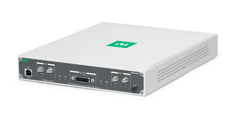
Real-World SDR Applications: 5G Research, Satellites, IoT and ADS-B
Where software defined radio actually earns its place: 5G and 6G waveform research, spectrum monitoring, weather satellite reception, GNSS work, LoRaWAN debugging, aircraft tracking over 1090 MHz, and reconfigurable instrument prototyping. A practical map from GSAS Micro Systems, an authorized Digilent engineering partner in India, with a framework for matching a USRP platform to the job.
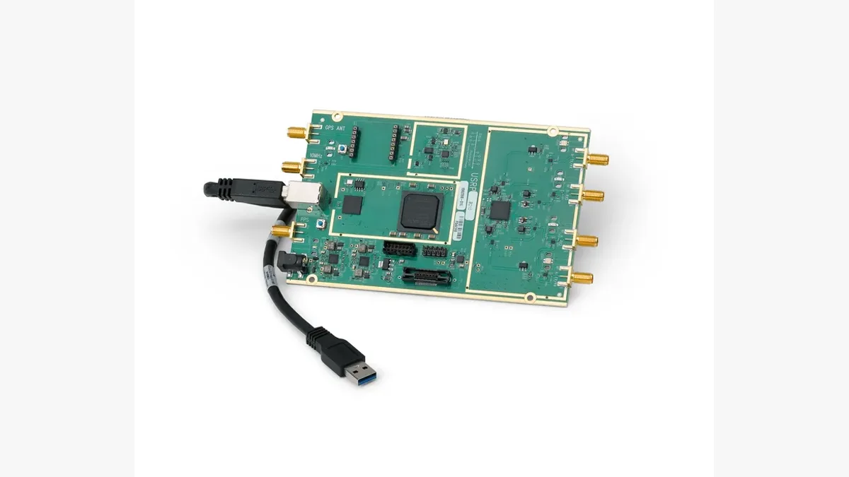
What Is Software Defined Radio (SDR)? A Practical Explainer for Indian Engineering Teams
Software defined radio moves the work of filtering, modulation and demodulation out of fixed hardware and into software running on processors and FPGAs. This explainer from GSAS Micro Systems covers what SDR is, how it differs from a traditional radio, what the signal chain looks like, why the FPGA matters, and how to pick a USRP radio in India.

ZedBoard FPGA-in-the-Loop: HDL Verifier vs HDL Coder
Teams asking for FPGA-in-the-Loop on a ZedBoard usually name HDL Coder and SoC Blockset. FIL is actually HDL Verifier. Here is the correct product split, the JTAG versus Ethernet decision, and the 2015-era advice that is still sending Indian teams down the wrong path.

AI Data Centers in India: Test, Measurement & Memory Boom
AI is a hardware supercycle. Every AI rack has to be designed, brought up, powered, fed with memory, and kept alive, and each of those is a test, measurement and memory problem. Here is the full engineering toolchain behind the AI data center, mapped to what Indian teams can buy today through GSAS.
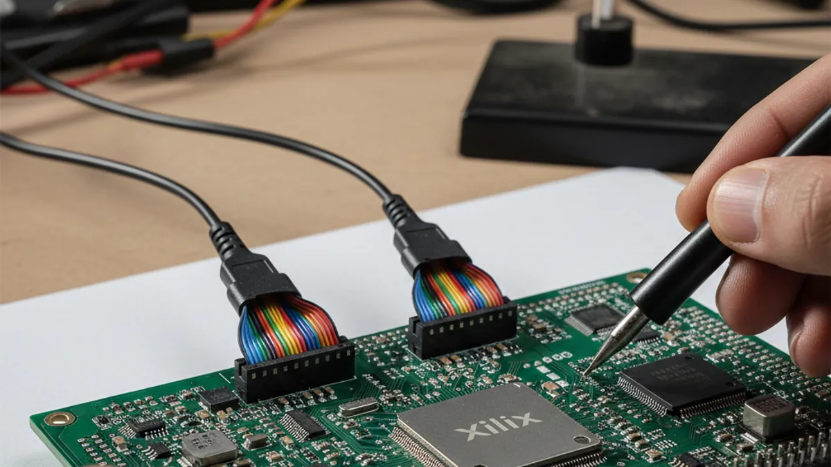
JTAG-HS3 vs HS2 FPGA Programming Cable: Boundary Scan, Production & Validation in India
A use-case guide to the Digilent JTAG-HS2 vs JTAG-HS3 FPGA programming cables for the engineers who actually rely on them, memory-validation bench teams, defence and aerospace FPGA production lines, and high-volume EMS boundary-scan test. Specs, IEEE 1149.1 structural test, production flash programming, and which cable to buy in India.

MCC USB DAQ Selection Guide for Indian Labs: USB-1808X vs USB-1608G vs MCC 118
Choosing an MCC USB data acquisition device for an Indian lab comes down to three questions: do you need simultaneous sampling, how many channels, and Raspberry Pi or PC? This guide compares the MCC USB-1808X, USB-1608G Series, and MCC 118 DAQ HAT.
Have an FPGA Design Challenge?
Whether you need an RTL design verified, a Zynq PS-PL system integrated, or an FPGA prototype for your next ASIC, our digital design engineers are ready.