
Semiconductor Design
From RTL to Silicon Validation.
Virtual prototyping, first-silicon bring-up, power optimization, and production test, tools for every stage of the semiconductor development lifecycle.
Semiconductor companies face unique development challenges that span the entire lifecycle from RTL design through silicon validation and production test. Whether developing Safety Elements out of Context (SEooC) for automotive or building high-performance application processors, teams need tools that bridge the gap between hardware design and software enablement. GSAS provides the debug, trace, measurement, and programming tools essential for semiconductor development.
J-Link PRO delivers the high-speed debug and trace connectivity required for first-silicon bring-up and software enablement, supporting Arm Cortex-M, Cortex-A, Cortex-R, and RISC-V architectures. Joulescope JS220 enables precision power profiling critical for validating power management IP and optimizing power states. PicoScope provides the high-resolution mixed-signal analysis needed for verifying chip-to-chip communication interfaces during board bring-up.
India’s semiconductor ecosystem is expanding rapidly with new design centers and fabrication initiatives. GSAS partners with leading semiconductor IP and EDA companies including Arm and Siemens EDA to deliver integrated toolchains that accelerate time-to-market while meeting the functional safety requirements increasingly demanded by automotive and industrial semiconductor customers.
Need help selecting tools for your project?
Our application engineers specialize in Semiconductor Design toolchain selection, from architecture through production.
What We Bring
GSAS Capabilities for Semiconductor Design
Beyond tools, engineering services, compliance consulting, and hands-on support tailored to Semiconductor Design teams.
Embedded Software Engineering
First-silicon bring-up and software enablement, BSP development, and debug and trace integration across Cortex-M, Cortex-A, Cortex-R and RISC-V targets.
Safety & Compliance Engineering
ISO 26262 SEooC for safety IP and hardware reliability analysis for silicon.
Test & Measurement Integration
Precision power profiling for power-management IP validation, and high-resolution mixed-signal analysis of chip-to-chip interfaces during board bring-up.
Training & Enablement
Xpedition PCB Layout workshops, Embedded Architecture deep-dives and custom corporate programmes for design centres.
Recommended Tools
Products for Semiconductor Design
Curated from our portfolio of authorized global partnerships, the tools that Semiconductor Design engineering teams use most.
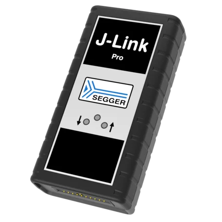
J-Link PRO
Professional JTAG/SWD debug probe with USB and Ethernet connectivity, supporting Arm Cortex-M/A/R and RISC-V architectures. India pricing and local support from GSAS.
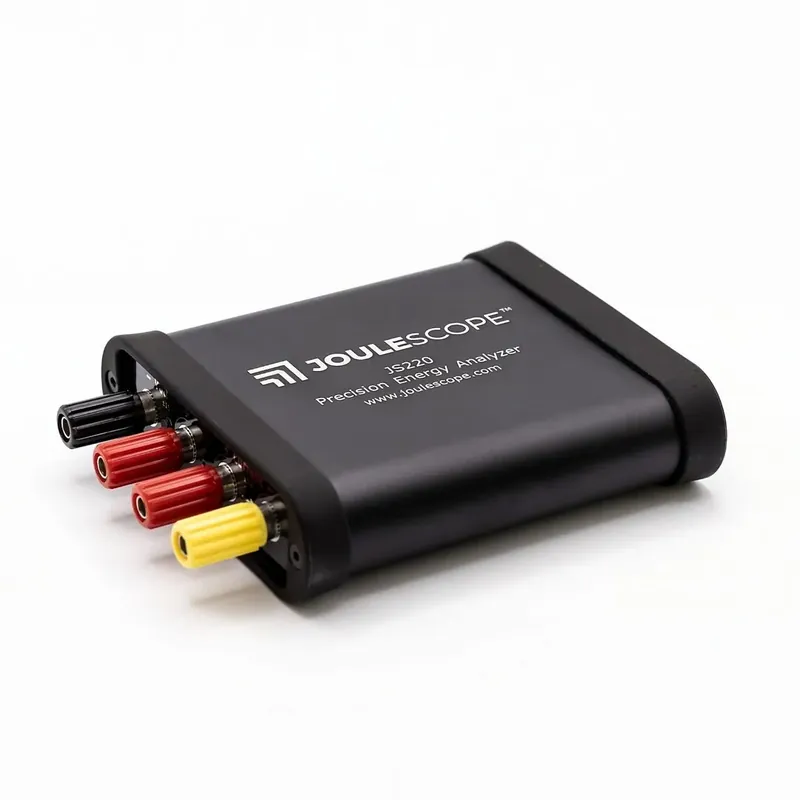
Joulescope JS220
Precision DC energy analyzer with 9-decade dynamic range for battery life optimization and power profiling. Available in India from GSAS with hands-on application engineering and local support.
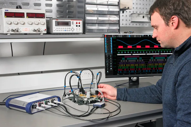
PicoScope 6000E
High-bandwidth USB oscilloscope spanning 300 MHz to 3 GHz bandwidth, FlexRes 8-to-12-bit resolution, and up to 4 GS deep memory. Authorized India partner, GSAS Micro Systems.
Calibre
Industry-standard IC physical verification and signoff platform, DRC, LVS, parasitic extraction, and pattern matching for advanced-node tapeout. Available in India from GSAS.
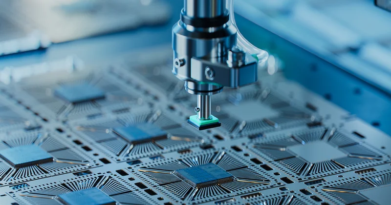
Tessent
Design-for-test (DFT) insertion, ATPG, BIST, diagnosis, and silicon lifecycle management for automotive and high-reliability ICs. Available in India from GSAS.

Solido
Statistical variation-aware simulation and library characterization for advanced-node analog/mixed-signal IC design. Available in India from GSAS.

Questa FPGA Essentials (QuestaSim FPGA Edition)
Questa FPGA Essentials (QuestaSim FPGA edition), the Siemens EDA FPGA simulation and verification bundle built on the Questa simulator, with UVM and mixed-language support and an optional RTL lint add-on. Available in India from GSAS, Siemens EDA authorized engineering partner.
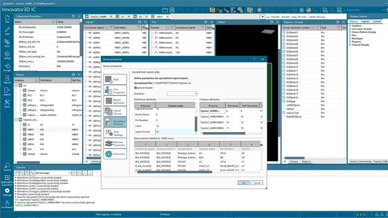
Innovator3D IC Layout
TSMC InFO-certified IC packaging layout tool for 2.5D/3D integration and advanced fan-out wafer-level packaging. Buy in India from GSAS with local support.
Compliance
Standards & Toolchain Mapping
Standards listed for Semiconductor Design, and the GSAS tools this site places against each. A chip shows a published qualification scope where one exists, and the bare standard name where none does.
ISO 26262 SEooC is listed in this page's standards set, but no tool in the table below carries a published qualification against it, and GSAS does not claim one. Whether this applies to a given programme depends on its scope, jurisdiction and certification basis.
| Tool | Applicable Standards |
|---|---|
| Klocwork (Perforce) | IEC 61508 up to SIL 4 |
| Perforce QAC | IEC 61508 up to SIL 4 |
| Arm Compiler for Embedded FuSa | IEC 61508 SIL 3 (qualified releases) |
| embOS-Safe (SEGGER) | IEC 61508 SIL 3 |
| TESSY (Razorcat) | IEC 61508 (T2 support tool) |
Blog
Latest Thinking: Semiconductor Design

India's EDA Moment: Why Design Tool Demand Is Growing, and the Engineering Careers It Creates
Electronic design automation is one of the few engineering markets where the global numbers and India's industrial policy are pointing the same direction at the same time. Here is what the published data actually says, which engineering roles the growth creates, and where GSAS Micro Systems fits as an authorized Siemens EDA engineering partner.

Calibre Vision AI: Bringing Order to DRC Debug at Advanced Nodes
Siemens EDA's Calibre Vision AI turns full-chip DRC debug from an unmanaged flood of violations into a tracked, filtered, hand-off-able workflow. What Signal status tracking, global filters and shareable workspaces mean for Indian SoC teams.
I3C FAQ for Firmware Teams: What the Bus Is, What Changes, and What You Need on the Bench
MIPI Alliance describes I3C as the successor to I2C, with legacy compatibility so that I3C and I2C devices can coexist on the same bus, a two-wire interface that supports in-band interrupts to reduce pin count, plus multi-controller support and dynamic addressing. This FAQ answers the questions firmware teams actually ask before adopting it.
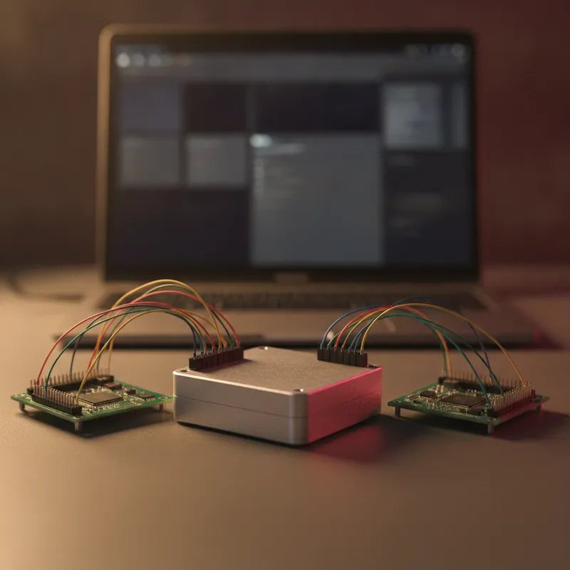
Running the Binho Supernova as an I3C Target: Emulating a Device Against Your Own Controller
Binho specifies the Supernova's I3C role as Controller or Target, which means the same adapter can stand in as the device under test rather than only driving one. That second direction is how a team validates its own I3C controller, its ENTDAA implementation and its interrupt handling, before the target silicon exists.
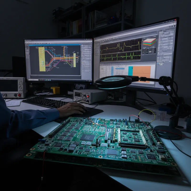
PicoScope Signal Integrity in India: USB 3.x, PCIe, DDR, and Ethernet-APL
How Indian SoC and board teams use PicoScope 6000E, PicoScope 9400A SXRTO, and PicoVNA 108 for USB 3, PCIe, DDR, and Ethernet-APL signal integrity work.
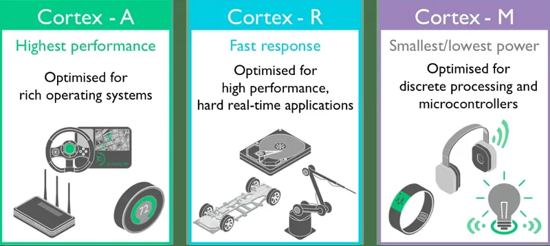
How to Choose an Arm Cortex Processor: A Selection Guide for Indian Embedded Teams
Choosing an Arm Cortex core is a decision about real-time determinism, memory architecture and toolchain, not about clock speed. This selection guide walks Indian embedded teams from workload to short list, including MCU vendors, toolchains and debug probes.

MIPI I3C Adoption in Indian Semiconductor Design Centers
MIPI Alliance lists I3C v1.0 as a 2016 release, and the design centres in Bengaluru and Hyderabad that build sensor hubs, camera interface modules and PMICs are where its adoption in India is concentrated. The practical constraint is rarely the specification; it is having bench instrumentation that can drive an I3C bus interactively during bring-up.
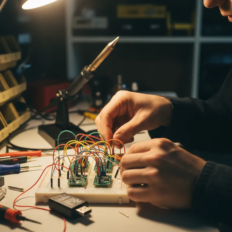
I3C Sensor Bring-Up with the Binho Supernova: Bus Scanning, Dynamic Addressing, CCC Commands, and IBI
I3C sensor bring-up is not an I2C bus scan with extra steps. Before the first register read you have to reset and run dynamic address assignment, read back each target's Provisioned ID, BCR and DCR, and configure events with CCCs. This guide walks that sequence on the Binho Supernova, which Binho specifies as an I3C Controller or Target at up to 12.5 MHz.
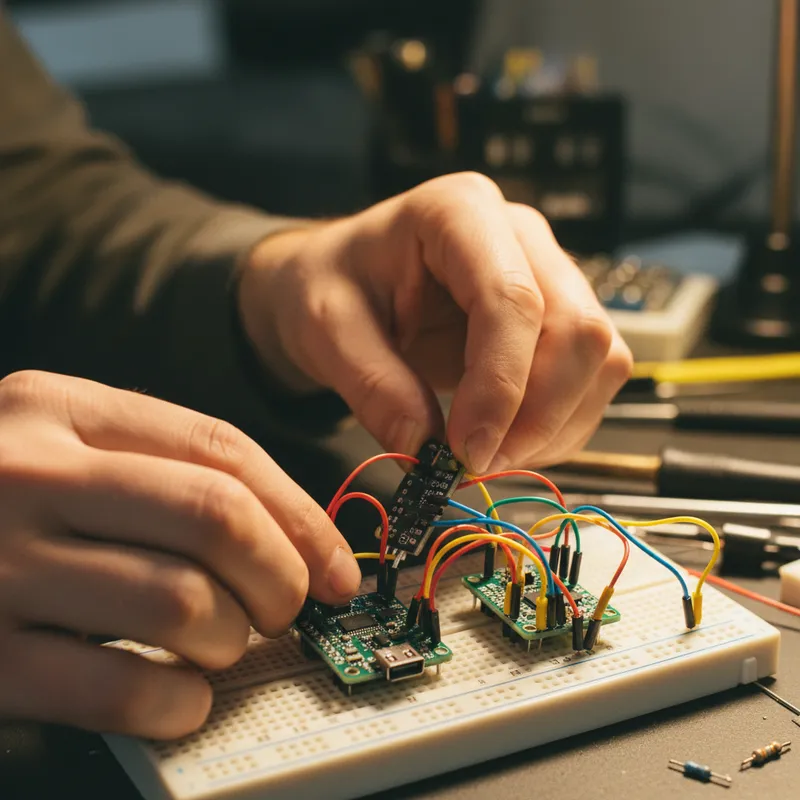
Binho Supernova: A Full MIPI I3C Exerciser for Firmware Teams
Binho specifies the Supernova for MIPI I3C spec versions v1.0, v1.1.1 and v1.2, up to 12.5 MHz, in SDR mode and HDR-DDR, with In-Band Interrupts, Hot-Join and all Common Command Codes, at 0.8 V to 3.3 V, and with an I3C role of Controller or Target. That combination is what makes interactive I3C bring-up practical on a bench rather than only on an FPGA prototype.

PCB Repair Guide: Detecting BGA Solder Joint Failures with VI Curve Analysis
How to use VI curve tracing to detect BGA solder joint failures, open balls, bridged pins, and cold joints, without X-ray equipment. A practical guide for Indian repair workshops.
DDR5 Signal Integrity Simulation with HyperLynx: Timing, Topology, and Compliance
DDR5 at 6400 MT/s demands pre-layout topology exploration and post-layout timing validation. Learn how HyperLynx SI helps semiconductor design teams in India simulate write leveling, DQ/DQS timing, and VrefDQ noise margins.

Signal Integrity for High-Speed PCB Design: A Practical Guide for Indian Hardware Teams
With DDR5, PCIe Gen5, and USB4, every multi-layer PCB is now a high-speed design. Here's how Indian hardware teams can avoid common signal integrity mistakes and ship boards that work on the first spin.
Ready to Build Your Semiconductor Design Toolchain?
Our application engineers have deep domain experience in Semiconductor Design. From tool selection to compliance consulting to production deployment, one ecosystem.