
 Siemens EDA
 Innovator3D IC Layout
IC PackagingTSMC InFO-certified IC packaging layout tool for 2.5D/3D integration and advanced fan-out wafer-level packaging. Buy in India from GSAS with local support.
Certification
TSMC InFO_oS, InFO_PoP
Package Types
2.5D, 3D, FOWLP, SiP, MCM
Automation
RDL routing, bump placement
Co-Design
NX integration
Output
GDSII, ODB++
Overview
About Innovator3D IC Layout
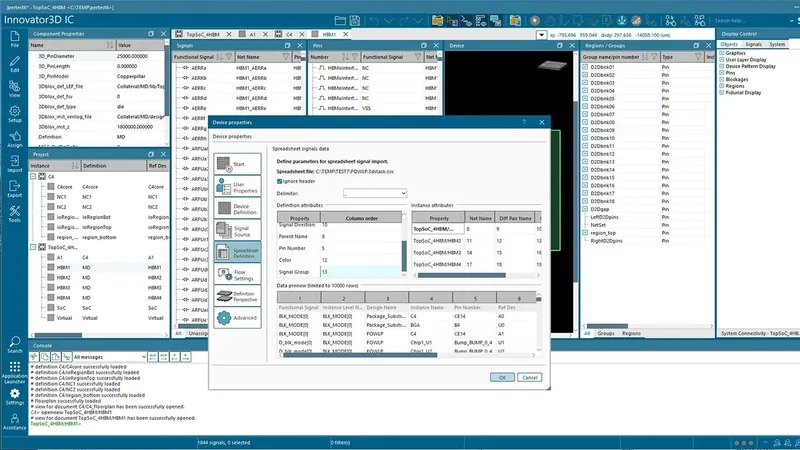
Innovator3D IC Layout is Siemens EDA’s advanced IC packaging layout tool, production-validated and certified by TSMC for InFO (Integrated Fan-Out) technologies including InFO_oS and InFO_PoP. As semiconductor design moves aggressively toward heterogeneous integration, chiplet-based architectures, and advanced packaging, Innovator3D provides the layout automation and foundry-certified design kit support needed to address 2.5D interposer, 3D stacking, fan-out wafer-level packaging (FOWLP), and system-in-package (SiP) designs. The tool bridges the traditional gap between IC design and packaging with unified layout capabilities that span from redistribution layer (RDL) routing to through-silicon via (TSV) planning.
2.5D interposer design with silicon bridge routing enables high-bandwidth die-to-die communication for chiplet architectures, while 3D die stacking with TSV planning supports vertical integration of logic and memory dies. Automated RDL routing, bump placement, and via generation from foundry-specific design rules and constraints accelerate layout of even the most complex packaging configurations. RDL routing automation handles the intricate redistribution layers that connect die pads to package-level I/O, managing thousands of routes across multiple RDL metal layers with full DRC awareness. Integrated design rule checking against foundry design kits catches violations during layout rather than after tapeout, providing immediate feedback on design compliance.
Fan-Out Wafer-Level Packaging (FOWLP) support addresses the growing demand for thin, compact packages with high I/O density, a critical technology for mobile SoCs, IoT devices, and wearables where traditional wire-bond and flip-chip packages cannot meet size and performance requirements. System-in-Package (SiP) integration enables layout of complete systems combining heterogeneous dies, passive components, and interconnect within a single package substrate, serving applications from advanced mobile platforms to automotive sensor fusion modules.
Support for chiplet-based SiP and multi-chip module (MCM) configurations addresses the growing demand for heterogeneous integration of compute, memory, and I/O chiplets, a key technology driver for AI accelerators, high-performance computing, and advanced mobile SoCs. Advanced substrate design for high-bandwidth memory (HBM) and chiplet architectures delivers the routing density and signal integrity needed for next-generation HBM3 and emerging HBM4 standards memory stacks interfacing with logic dies through silicon interposers.
Bi-directional integration with Siemens NX enables mechanical co-design with thermal interface material and stress consideration, ensuring that packaging designs meet both electrical and mechanical requirements. Integration with Xpedition enables package-to-board co-design, ensuring consistent signal integrity and power delivery from the die through the package substrate to the PCB, eliminating the traditional disconnect between IC packaging and board-level design teams. From simple BGA packages to advanced TSMC InFO designs with thousands of bumps and RDL layers, Innovator3D scales across the full complexity spectrum with foundry-specific tutorials and all-in-one (AIO) packages for rapid adoption.
Key Features
- TSMC InFO Certified: Production-validated for TSMC Integrated Fan-Out technologies including InFO_oS and InFO_PoP. Layout automation from TSMC design kit rules.
- 2.5D Interposer Design: Silicon bridge routing for high-bandwidth die-to-die communication in chiplet architectures. Supports passive and active interposer configurations.
- 3D Die Stacking: Through-silicon via (TSV) planning for vertical integration of logic and memory dies. Full 3D stackup visualization and DRC.
- Fan-Out Wafer-Level Packaging: FOWLP layout for thin, high-density packages serving mobile SoCs, IoT, and wearable applications.
- System-in-Package Integration: Complete SiP layout combining heterogeneous dies, passive components, and interconnect within a single package substrate.
- RDL Routing Automation: Automated redistribution layer routing across multiple RDL metal layers with full foundry DRC awareness. Handles thousands of routes efficiently.
- HBM and Chiplet Substrates: Advanced substrate design for high-bandwidth memory stacks and chiplet architectures with the routing density modern HBM3 and emerging HBM4 standards interfaces demand.
- Xpedition Package-to-Board Co-Design: Integration with Xpedition for consistent signal integrity and power delivery from die through package to PCB.
- Electro-Mechanical Co-Design: IC package design bridging ECAD and MCAD domains. Thermal interface material and mechanical stress consideration.
- Multi-Die Integration: Layout tools for chiplet-based designs, system-in-package (SiP), and multi-chip module (MCM) configurations.
- DRC Integration: Integrated design rule checking against foundry design kits. Catch violations during layout, not after tapeout.
- NX Integration: Bi-directional integration with Siemens NX for mechanical co-design of IC packages and thermal analysis.
- Scalable Complexity: From simple BGA packages to advanced TSMC InFO and interposer designs with thousands of bumps and RDL layers.
Platform Capabilities
| Capability | Detail |
|---|---|
| Foundry Certification | TSMC InFO_oS, InFO_PoP (production-validated) |
| Package Types | 2.5D interposer, 3D stacking, FOWLP, SiP, MCM |
| 2.5D/3D | Silicon bridge routing, TSV planning, die stacking |
| Automation | RDL routing, bump placement, via generation |
| Substrate Design | HBM, chiplet architectures, high-density interconnect |
| DRC | Foundry design kit rule checking |
| Co-Design | Xpedition (package-to-board), NX (mechanical/thermal) |
| Output | GDSII, ODB++ for manufacturing |
| Training | Foundry-specific tutorials and AIO packages |
Target Applications
- Advanced IC Packaging: TSMC InFO wafer-level packaging for mobile SoCs, high-performance computing, and AI accelerators. Production-validated design kits ensure first-pass silicon success.
- Chiplet Integration: Multi-die system-in-package layout for heterogeneous integration of compute, memory, and I/O chiplets with silicon bridge routing and TSV planning.
- High-Performance Computing: 2.5D interposer designs for HPC and data center applications with high-bandwidth memory (HBM) integration and advanced substrate routing.
- Fan-Out Packaging: FOWLP designs for mobile, IoT, and wearable applications demanding thin profiles, high I/O density, and excellent thermal performance.
- Automotive SoC Packaging: Advanced packaging for automotive processors and sensor fusion ICs with thermal management requirements and package-to-board co-design.
Why GSAS for Innovator3D IC Layout
GSAS supports Indian semiconductor packaging teams with Innovator3D IC Layout licensing, foundry-specific configuration, and technical consulting. Our field application engineers help with TSMC InFO design kit setup, RDL routing automation, and integration with your NX mechanical design and Xpedition board-level design workflows. Contact us about licensing, training packages, and getting started with advanced IC packaging layout.
GSAS Micro Systems is an authorized Siemens EDA partner in India, providing Innovator3D IC Layout licensing, foundry design kit configuration, and technical support for semiconductor packaging teams working on 2.5D/3D integration and advanced fan-out technologies.
Buy Innovator3D IC Layout in India: GSAS India-Wide Support
GSAS provides Innovator3D IC Layout with INR invoicing, local FAE support, and Siemens maintenance and support across India:
- Bengaluru: Semiconductor design centres and OSAT companies working on 2.5D interposer, fan-out WLP, and advanced SiP packaging for mobile SoCs and AI accelerators
- Hyderabad: Defence semiconductor packaging teams, growing fabless design community, and IC packaging R&D groups working on heterogeneous integration
- Chennai: Automotive semiconductor packaging for ADAS and powertrain SoCs, and OSAT facilities supporting advanced packaging technologies
- Pune: Automotive IC packaging R&D and industrial semiconductor companies designing SiP modules for vehicle electronics
- Mumbai: Semiconductor packaging teams serving telecom and data centre IC programs
- Delhi NCR: Defence and space semiconductor packaging groups designing radiation-hardened IC packages and multi-chip modules
- Coimbatore: Industrial semiconductor companies exploring advanced packaging for power management ICs
- Visakhapatnam: Naval defence electronics packaging teams and medical device semiconductor companies
- Vadodara: Power semiconductor packaging teams and industrial IC design groups
- Kolkata: Eastern India semiconductor design teams and academic research groups working on advanced packaging
Contact sales@gsasindia.com or call +91 80 6590 1783 for evaluation licenses, TSMC InFO design kit configuration, and foundry packaging flow setup.
Blog
Siemens EDA Insights

India's EDA Moment: Why Design Tool Demand Is Growing, and the Engineering Careers It Creates
Electronic design automation is one of the few engineering markets where the global numbers and India's industrial policy are pointing the same direction at the same time. Here is what the published data actually says, which engineering roles the growth creates, and where GSAS Micro Systems fits as an authorized Siemens EDA engineering partner.

AI and Complexity Are Redrawing EDA: Siemens on the Trillion-Transistor Era
Siemens argues that chip complexity has outgrown siloed design and that the lines between chip, package and board can no longer be drawn. GSAS summarises the Industry Forward podcast episode and sets out what it changes for design teams in India: verify across the chip-to-board boundary before layout, not after the prototype.

Calibre Vision AI: Bringing Order to DRC Debug at Advanced Nodes
Siemens EDA's Calibre Vision AI turns full-chip DRC debug from an unmanaged flood of violations into a tracked, filtered, hand-off-able workflow. What Signal status tracking, global filters and shareable workspaces mean for Indian SoC teams.
Related products
More from Siemens EDA
All Siemens EDA products →
Xpedition Package Designer
IC package substrate and interposer layout for BGA, flip-chip, fan-out, and 2.5D/3D heterogeneous integration. Available in India from GSAS.
View Xpedition Package Designer →
Calibre
Industry-standard IC physical verification and signoff platform, DRC, LVS, parasitic extraction, and pattern matching for advanced-node tapeout. Available in India from GSAS.
View Calibre →
Solido
Statistical variation-aware simulation and library characterization for advanced-node analog/mixed-signal IC design. Available in India from GSAS.
View Solido →Interested in Innovator3D IC Layout?
Get pricing, an evaluation unit, or a technical consultation from our application engineers.