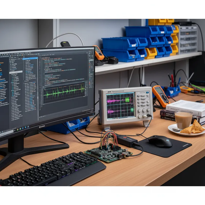
Electronic design automation is an unglamorous phrase for a fairly dramatic idea: that almost every chip and almost every circuit board in the world is now designed inside software, and that comparatively few engineers in India have deep working command of it.
That gap, between how much design work India is taking on and how many engineers can actually run the tools that design work depends on, is the most interesting thing happening in our corner of the industry right now. It is also the reason this page exists. We get asked about it by customers planning headcount, by engineers deciding what to specialise in, and by graduates who have heard “semiconductor” in the news and want to know where an actual job sits.
What follows is the published evidence, with the sources named, and an honest note about where the data stops.
What the global EDA numbers actually say
The most direct measurement of the design tools market comes from the Electronic Design Market Data report, published quarterly by the ESD Alliance, a SEMI Technology Coalition. It collects revenue data from both public and private companies and covers EDA, semiconductor IP and services.
In its most recent published quarter, the numbers are these:
- Electronic System Design industry revenue increased 12.7% to $5,747.8 million in the first quarter of 2026, from the $5,098.3 million registered in the first quarter of 2025. The four-quarter moving average rose 10.3%.
- Computer-Aided Engineering revenue increased 15.5% to $2,018.4 million. This is the simulation and verification category, and it grew faster than the market as a whole.
- Semiconductor IP revenue increased 14.1% to $2,332.5 million.
- IC Physical Design and Verification revenue increased 8.3% to $751.3 million.
- Printed Circuit Board and Multi-Chip Module revenue rose 4.8% to $419.2 million.
- Services revenue increased 6.5% to $226.4 million.
By region, Asia Pacific procured $2,264.4 million of electronic system design products and services in Q1 2026, a 17.7% increase, with a four-quarter moving average up 14.5%. That was the fastest growth of any major reporting region alongside EMEA, and it puts APAC within touching distance of the Americas, which remained the largest reporting region at $2,433.8 million.
Here is the honest caveat, and it matters more than the headline. The EDMD report segments revenue into Americas, EMEA, Japan and APAC. It does not break India out separately. India sits inside that APAC figure along with China, Taiwan, Korea and the rest of the region, so the 17.7% is regional growth, not an India growth rate. Anyone quoting an APAC number as an India number is overstating what the source supports. We would rather tell you where the data stops than pad the story.
For the India-specific picture, you have to go to Indian sources.
Why the demand curve bends towards India
India’s design tool demand is not a market accident. It is the downstream consequence of an explicit industrial policy, and the government publishes its own numbers.
According to the Press Information Bureau backgrounder on India Semiconductor Mission 2.0, published 7 February 2026:
- India Semiconductor Mission 1.0 was approved by the Union Cabinet in December 2021 and is supported by an incentive framework of Rs 76,000 crore, offering fiscal support of up to 50 per cent for silicon fabs, compound semiconductor facilities, assembly and testing units, and chip design.
- As of December 2025, 10 projects with a total investment of Rs 1.60 lakh crore have been approved across 6 states, covering silicon fabrication, silicon carbide fabs, advanced and memory packaging, and specialised assembly and testing infrastructure.
- On the market itself, the backgrounder cites industry estimates putting the Indian semiconductor market at about $38 billion in 2023, $45 billion to $50 billion in 2024 to 2025, and an expected $100 billion to $110 billion by 2030. Note that this is the semiconductor market, not the EDA market. The two move together, but they are not the same number.
- By 2029, India is expected to achieve the capability to design and manufacture chips required for nearly 70 to 75 per cent of domestic applications, with the next phase under Semicon 2.0 targeting a roadmap to 3-nanometre and 2-nanometre technology nodes.
- Union Budget 2026-27 made a provision of Rs 1,000 crore for ISM 2.0 for FY 2026-27, with what the backgrounder describes as a strong emphasis on industry led research and training centres to create a future ready skilled workforce.
The single most EDA-relevant figure, though, comes from a different release. In the Press Information Bureau release on the Design Linked Incentive Scheme, dated 22 August 2025, the Ministry of Electronics and IT states that the government has sanctioned 23 chip-design projects under the DLI Scheme, and that 72 companies have gained access to the industry-standard Electronic Design Automation (EDA) tools for their chip design projects.
Read that last sentence the way a hiring manager reads it. Seventy-two companies now have tool access for chip design work. Tool access is necessary and completely insufficient on its own. Every one of those seats needs an engineer who can drive it, a methodology that survives the second project, and somebody who knows what to do when a simulation disagrees with the bench.
That is the actual shape of the opportunity. India is not short of EDA licences. It is short of EDA fluency.
The jobs this creates, and what they are called
The EDMD report also tracks employment at the companies that contribute data, and the trend there is unambiguous: the companies tracked in the report employed 72,544 people globally in Q1 2026, a 12.6% increase over the Q1 2025 headcount of 64,403, and up 1.1% compared to Q4 2025. Double digit headcount growth in a tooling industry is a leading indicator, because tool vendors hire ahead of the design activity they expect to support.
That is the vendor side. On the user side, in India, the roles that open up when a company takes on serious design work fall into a small number of recognisable families. We see all of them across our customer base:
- PCB layout and design engineering. Constraint-driven layout, stack-up, high-density interconnect, and the discipline of getting a complex board right the first time rather than the third.
- Signal integrity and power integrity. Pre-layout topology exploration, post-route verification, channel simulation, power distribution network analysis. This is the specialisation that scales fastest as interface speeds rise, and it remains one of the hardest roles in India to fill.
- Design verification. Functional verification of FPGA and ASIC designs, testbench architecture, constrained-random methodology, coverage closure. The CAE growth figure above is largely this work being bought.
- CAD, methodology and tool administration. The people who own the library, the constraint templates, the reuse blocks and the release flow. Under-glamorised, and the reason some teams ship twice as fast as others with identical tools.
- Application engineering. Engineers who know a toolchain deeply enough to get somebody else unstuck in it. This is the role GSAS itself hires for most often.
None of these are entry-level in the sense of being learnable from a course alone. All of them are learnable on real projects, which is precisely why the tool access story above matters.
What the work looks like inside the tools
Abstractions about market growth are easy. It is more useful to say what an engineer in these roles actually opens in the morning. Across the Siemens EDA portfolio, which is the design flow we support most deeply, three tools carry most of that daily work.
Xpedition is where board design happens. The current generation is AI-infused PCB design software with sketch routing, cloud DFM and token-based signal integrity add-ons, which in practice means a layout engineer spends less time on the mechanical majority of routing and more on the decisions that genuinely need judgement: clock distribution, return paths, high-speed pairs, mechanical conflict. For a team scaling from two layout engineers to six, the constraint and reuse model matters more than any single feature, because it is what stops project seven from starting at the same place as project one.
HyperLynx is the verification half of that flow: a unified PCB verification platform covering signal integrity, power integrity, electrical DRC, stack-up design and integrated electromagnetic solvers, with IBIS-AMI channel simulation and support across DDR3 through DDR5 and LPDDR3 through LPDDR5. This is the tool that turns “we think the DDR interface will close” into evidence before the board is fabricated. A respin avoided on a high-speed design is measured in months, not rupees.
Questa FPGA Essentials covers FPGA simulation and verification, built on the Questa simulator with UVM and mixed-language support and an optional RTL lint add-on. For the many Indian teams whose first serious verification investment is on the FPGA side rather than full ASIC scale, this is usually where the methodology conversation starts.
The through-line is that all three reward depth. An engineer who has spent two years genuinely inside one of them is more valuable than one who has skimmed six, and the market currently pays accordingly.
Where GSAS sits in this
GSAS Micro Systems is an authorized Siemens EDA engineering partner in India. To be precise about it, because precision here is worth more than puffery: we are one of several Siemens EDA partners serving this market, not the only one, and we do not claim otherwise. GSAS is a value added distributor/reseller for these products, and we have a dedicated FAE team ready to help you with custom built solutions matching your needs. The distinction is not branding. It is what we are organised to do.
What that means operationally is that our team includes layout, signal integrity and verification engineers who have spent careers inside these tools, and our support model is built around how Indian teams actually adopt EDA rather than how a licence is transacted: structured onboarding, reuse-library setup using your own circuitry, constraint migration from whatever flow you are on today, and engineering support after go-live from offices in Bengaluru, Hyderabad, Chennai, Pune, Mumbai and Delhi NCR. The full Siemens EDA portfolio we cover is set out on the Siemens EDA partner page.
GSAS has been an embedded engineering partner in India since 2010, and an authorized Siemens EDA engineering partner since 2026. The longer half of that is where we watched Indian design teams grow, stall, migrate tools and occasionally learn the expensive way that a licence is not a capability. Most of what we know about EDA adoption in India we learned from the projects that went sideways, not the ones that went smoothly.
If you are building a career in this
The reason this piece exists in the first place is that the question keeps arriving from two directions at once.
If you are hiring, the constraint you will hit is not tool budget. It is finding engineers who can take a constraint set seriously, and that is a training problem with a long lead time. Start it before the project that needs it.
If you are an engineer deciding where to go deep, signal and power integrity, verification methodology, and design-for-manufacture are the three specialisations where India currently has far more demand than supply, and where the work does not get commoditised quickly. All three are learnable, none are learnable quickly, and the compounding is real.
We hire into exactly these roles, and our openings are listed on the GSAS careers page. If nothing there matches and you work in this area anyway, write to us regardless. Engineers who can explain what went wrong on a difficult board are rarer than engineers who can list tools on a CV, and we have made room for the former before.
Sources
- ESD Alliance, a SEMI Technology Coalition, Electronic Design Market Data report, “ESD Alliance Reports Electronic System Design Industry Posts $5.7 Billion in Revenue in Q1 2026”, 13 July 2026. PR Newswire release
- Press Information Bureau, Government of India, PIB Backgrounder, “India Semiconductor Mission 2.0”, 7 February 2026. https://www.pib.gov.in/PressReleasePage.aspx?PRID=2224839®=3&lang=1
- Press Information Bureau, Ministry of Electronics and IT, “Government pushes semiconductor design innovation with the Design Linked Incentive (DLI) Scheme”, 22 August 2025. https://www.pib.gov.in/PressReleasePage.aspx?PRID=2159727®=3&lang=2
Also appears in:
Interested in Siemens EDA tools?
Talk to our application engineers for personalized tool recommendations.
More from Siemens EDA
View all →
AI and Complexity Are Redrawing EDA: Siemens on the Trillion-Transistor Era
13 Sept · 6 min

Calibre Vision AI: Bringing Order to DRC Debug at Advanced Nodes
24 Aug · 4 min

Siemens EDA EBS Expert Series: 6 Free PCB Design Webinars (Jul-Aug 2026)
20 Jul · 8 min

AI Data Centers in India: Test, Measurement & Memory Boom
4 Jun · 14 min

Emulating Processor Power for Thermal Testing: Why Constant Power
7 Oct · 7 min

CRPS and Rack Power Supply Testing: The Six Tests That Matter
7 Oct · 7 min