
Hardware Design
Hardware Design & PCB Engineering
Schematic capture through production-ready Gerber output. High-speed layout, signal integrity, power delivery, DFM review, plus turn-key product development from concept to certified production. Delivered by a team that designs its own hardware.
What We Do
Hardware Engineering Services in India
Six engineering disciplines covering the full hardware product lifecycle, from schematic architecture through production support and field failure analysis.
Schematic Capture & Design
Complete schematic design from system architecture through production-ready netlists. Power tree design, component selection, design rule validation, and Bill of Materials optimisation for cost and availability.
Multi-layer PCB Layout
High-density PCB layout up to 20+ layers, controlled impedance routing, high-speed differential pairs, power plane design, via optimisation, and DRC-clean Gerber output. From 2-layer prototypes to 24-layer production boards.
Signal Integrity & Power Integrity
Pre-layout and post-layout SI/PI analysis, reflection analysis, crosstalk simulation, power delivery network impedance, decoupling capacitor optimisation, and eye diagram validation for high-speed interfaces.
DFM & DFA Review
Design for Manufacturability and Design for Assembly review, ensuring your design can be reliably produced at scale. Padstack optimisation, solder paste aperture review, testability analysis, and fabrication constraint validation.
Turn-key Product Development
End-to-end product development from concept through certified production, system architecture, schematic, layout, prototype build, testing, certification support, and production handoff with complete documentation.
Production Support
Ongoing production engineering support, ECO management, component obsolescence mitigation, re-spin management, yield optimisation, and field failure analysis for deployed products.
Need help with hardware design?
Our hardware engineers specialize in schematic capture, multi-layer PCB layout, signal integrity, and turn-key product development.
Domain Expertise
Industries We Design For
Production-proven hardware across defence, industrial, and embedded platform domains. Every board listed here was designed, built, and shipped by GSAS from Bangalore.
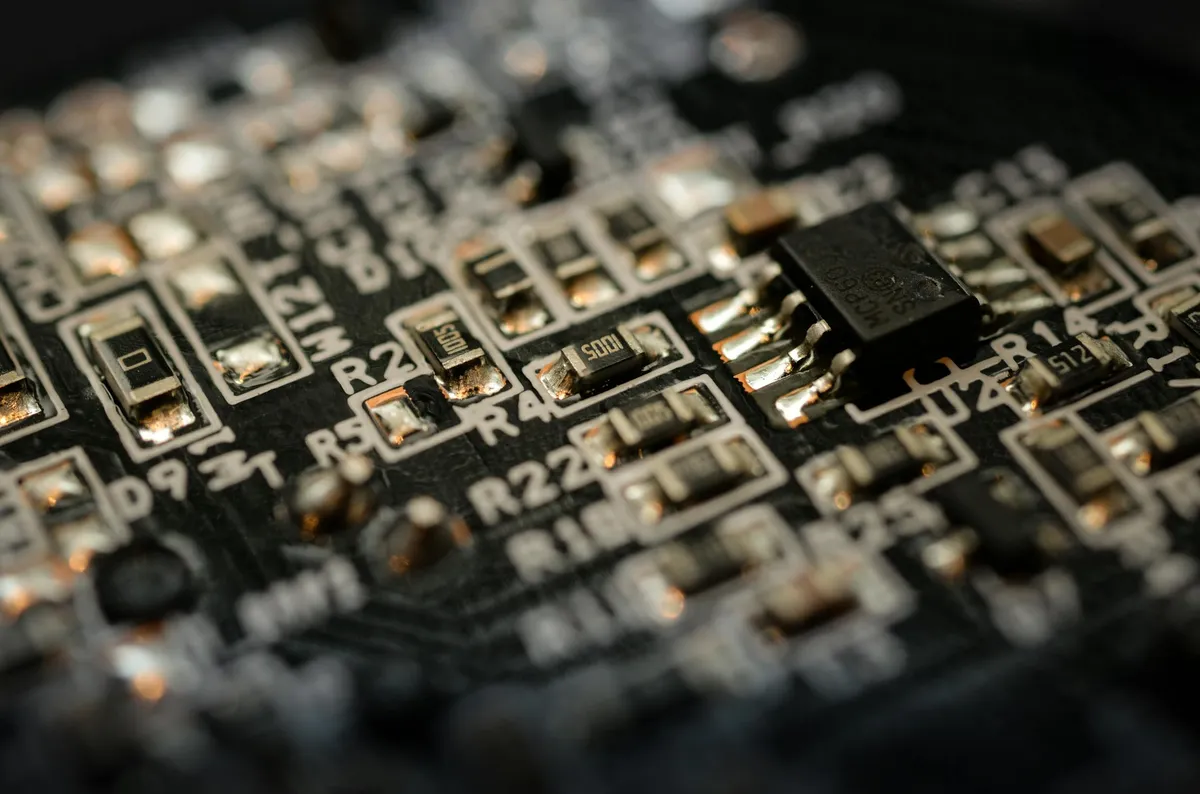
Defence & Aerospace
MIL-STD designStar sensors, sun sensors, data acquisition modules, missile prototyping boards. MIL-STD compliance and defence-grade PCB design for Indian defence programmes.

Industrial & IoT
Production hardwareHotel automation modules, PCI-DIO data acquisition cards, connected sensor platforms, and edge computing hardware for production environments.
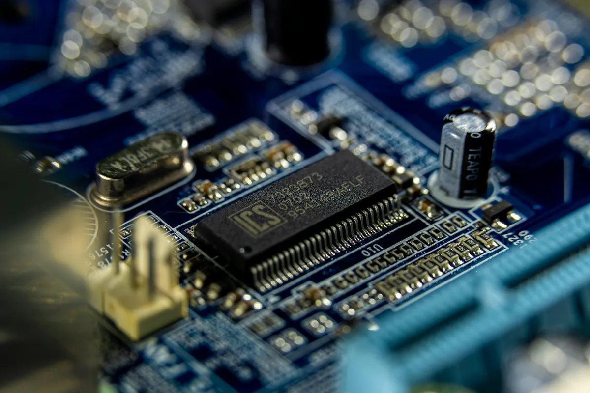
Embedded Platforms
Arm evaluation platformsArm-based evaluation boards and development kits, LPC 1768 (Cortex-M3) and LPC 2929 (ARM9) platforms used across Indian engineering labs.
Our Products
GSAS Product Range
Hardware designed, built, and shipped from Bangalore. These are not partner products, they are GSAS-engineered products used by teams across India.
Digital Microscopes
2MP portable to 4K UHD autofocus, PCB inspection, QC, and rework
View microscopes →ARM Development Boards
Cortex-M3 (LPC1768) and ARM9 (LPC2929) evaluation platforms
View boards →Microprocessor Trainers
8085, 8086/8088, and 8051 trainer kits for engineering education
View trainers →Peripheral Study Cards
8251/8253, 8255, 8259, 8279, plug-in IC training modules
View study cards →Interface Modules
Analog, display, input, and motor control peripheral boards
View modules →Board Diagnostics (FADOS)
FADOS circuit board testers, assembled by GSAS for ProT Ar-Ge
View FADOS →Portfolio
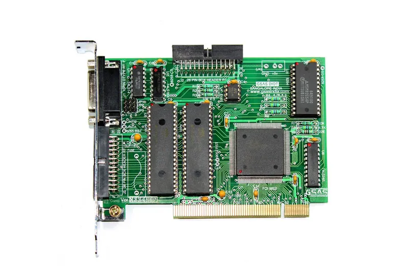
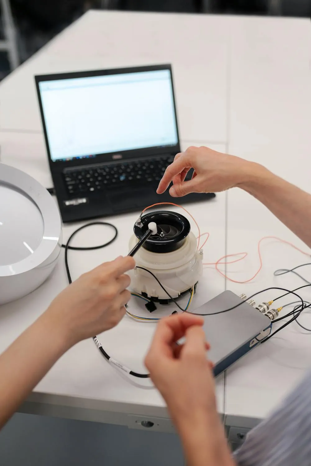
Hardware We Have Designed & Shipped
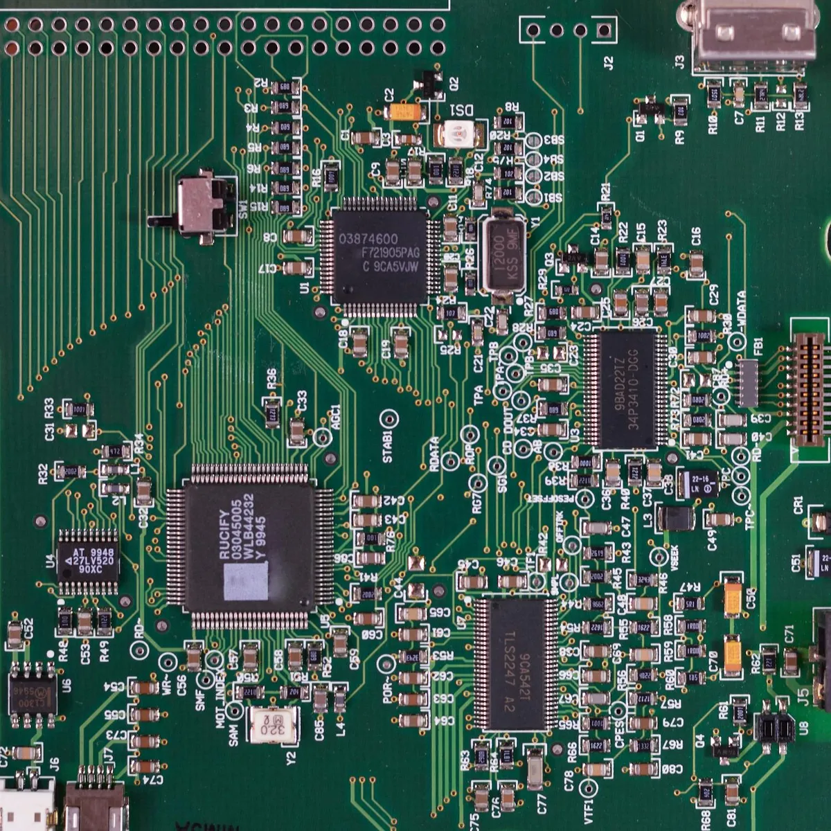
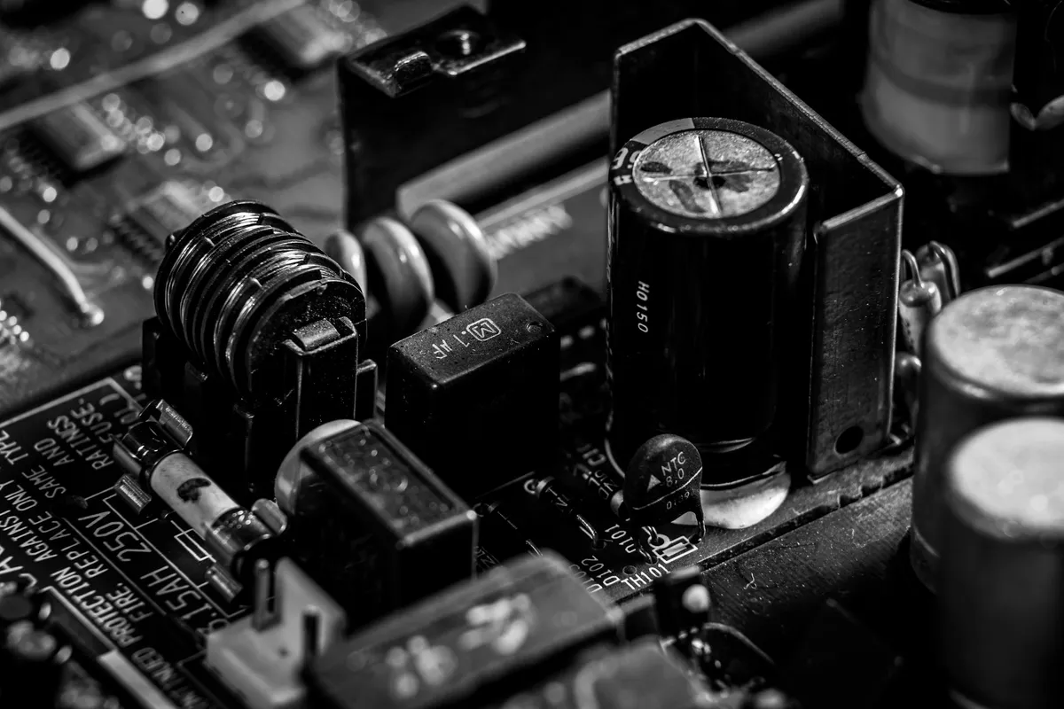
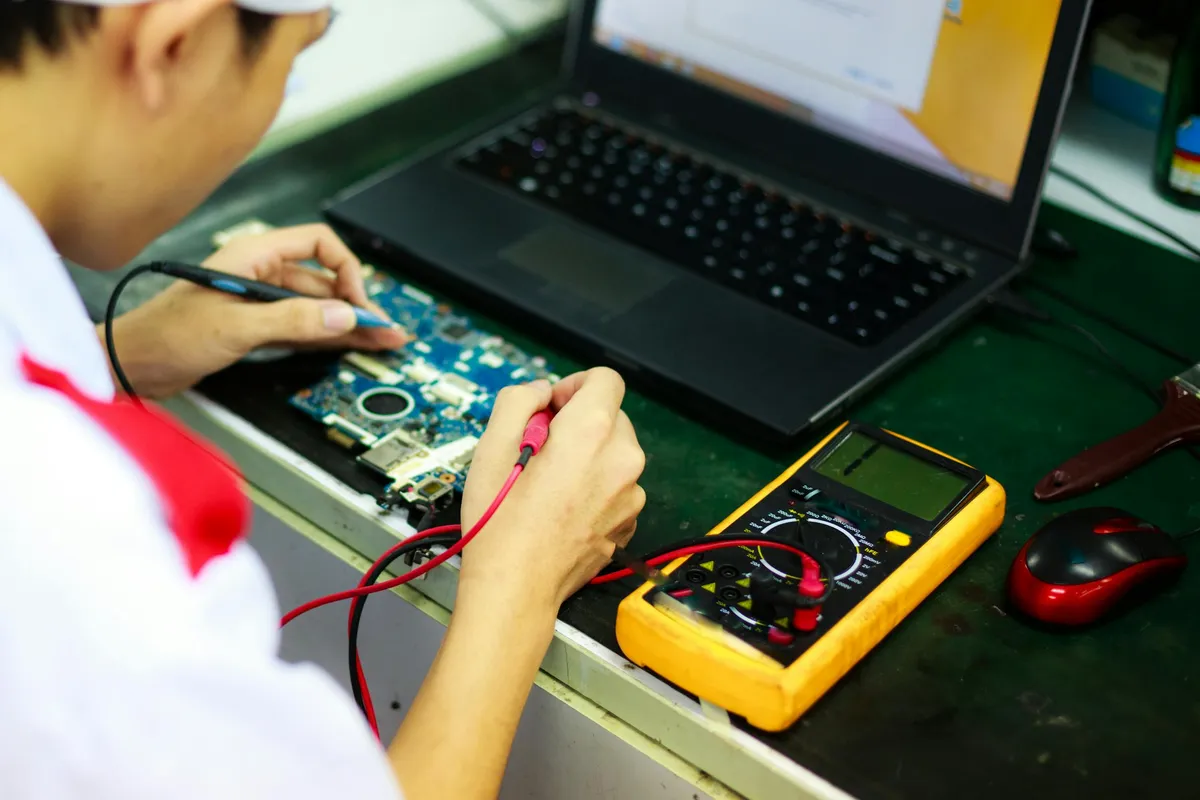
Real boards, real products, real engineering, designed and manufactured by GSAS in Bangalore since 2010.

Toolchain
PCB Design Tools We Use & Distribute
The Siemens EDA platform is our primary PCB design toolchain. We use these tools in our own hardware projects and distribute them across India with local application engineering support.

 Siemens EDA
 Xpedition Enterprise
Enterprise PCB design platform with integrated SI/PI analysis, constraint-driven routing, and team design collaboration for complex multi-layer boards.
View product →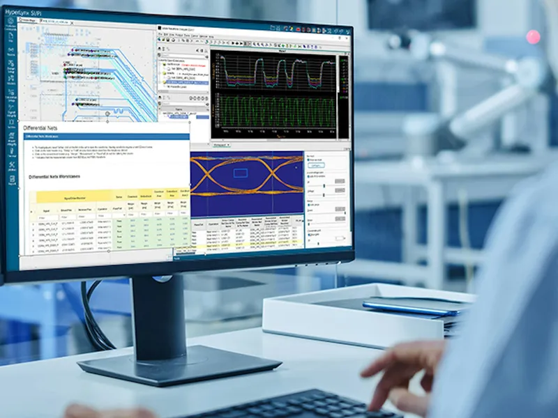 Siemens EDA
 HyperLynx
Unified signal integrity, power integrity, and electrical DRC, catch high-speed layout issues, PDN violations, and EMC problems before fabrication.
View product →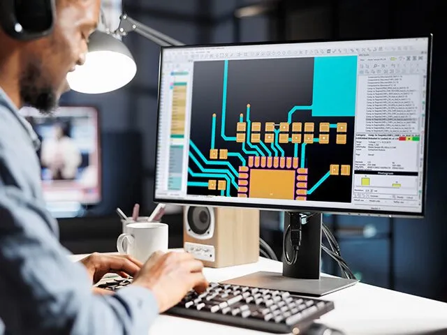 Siemens EDA
 Valor NPI
New Product Introduction analysis, automated DFM checks, panelisation review, and manufacturing process validation before sending to fabrication.
View product →Why GSAS
A Design House, Not a Body Shop

GSAS Micro Systems, Company Introduction
Boards Shipped
We do not just design PCBs, we manufacture and ship GSAS-branded hardware products used across India.
Enterprise Toolchain
We design on Xpedition, the same tools we supply and support. Battle-tested, not theoretical.
Mission-Critical Track Record
Defence programme work including star sensors for satellites and data acquisition for strategic weapons systems.
Blog
Hardware Design Insights

India's EDA Moment: Why Design Tool Demand Is Growing, and the Engineering Careers It Creates
Electronic design automation is one of the few engineering markets where the global numbers and India's industrial policy are pointing the same direction at the same time. Here is what the published data actually says, which engineering roles the growth creates, and where GSAS Micro Systems fits as an authorized Siemens EDA engineering partner.

AI and Complexity Are Redrawing EDA: Siemens on the Trillion-Transistor Era
Siemens argues that chip complexity has outgrown siloed design and that the lines between chip, package and board can no longer be drawn. GSAS summarises the Industry Forward podcast episode and sets out what it changes for design teams in India: verify across the chip-to-board boundary before layout, not after the prototype.

Calibre Vision AI: Bringing Order to DRC Debug at Advanced Nodes
Siemens EDA's Calibre Vision AI turns full-chip DRC debug from an unmanaged flood of violations into a tracked, filtered, hand-off-able workflow. What Signal status tracking, global filters and shareable workspaces mean for Indian SoC teams.

Siemens EDA EBS Expert Series: 6 Free PCB Design Webinars (Jul-Aug 2026)
Siemens EDA is running six free EBS Expert Series webinars from 22 July to 27 August 2026, covering HyperLynx PI DC Drop analysis, Xpedition DRC, Xpedition EDM and PLM integration, EDX, and Starpoints/Tiebars net shorting. GSAS, an authorized Siemens EDA engineering partner in India, is highlighting all six for Indian PCB design teams.

AI Data Centers in India: Test, Measurement & Memory Boom
AI is a hardware supercycle. Every AI rack has to be designed, brought up, powered, fed with memory, and kept alive, and each of those is a test, measurement and memory problem. Here is the full engineering toolchain behind the AI data center, mapped to what Indian teams can buy today through GSAS.
AI and Intelligent Automation in PCB Design: How Siemens Xpedition Removes the Work That Slows Indian Teams Down
Siemens' own engineers describe a 'productivity paradox' in PCB design: the tools have never been more capable, yet throughput has not kept pace. This is how AI, intelligent automation, design reuse and connected data continuity in Xpedition Standard close that gap, and what it means for PCB design teams in Bengaluru, Pune, Chennai, Hyderabad, Mumbai and Delhi NCR.
Have a Hardware Design Challenge?
Whether you need a PCB designed, a product developed from concept to production, or signal integrity analysis on a high-speed layout, our hardware engineering team in Bengaluru is ready.