
Ethernet
IC9 (DP83848CVV)
DP83848CVV 10/100 PHY on an RMII bus into an RJ45 with integrated magnetics (J13); 49.9 Ω pair terminations.
- IC9
- J13
First board in the GSAS Genesis series
An STM32F407 processor board seats on the Bridge's two 50-pin morpho headers, J1 and J2. Around it, the Bridge wires and terminates eight peripherals: Ethernet, three RF module slots, CAN, stepper drive, storage, sensing, power, and a display and keypad HMI.
Designed in Bengaluru by the engineers who needed it first.
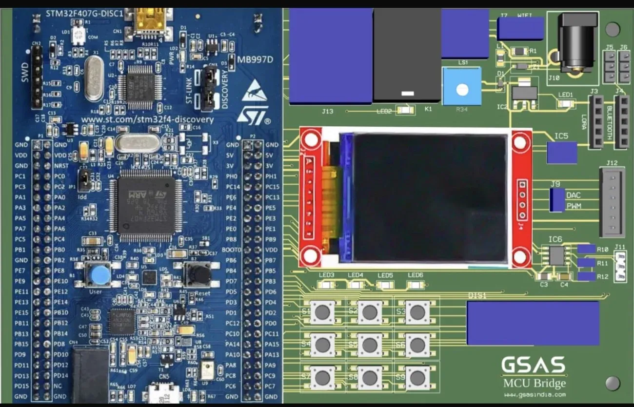
Genesis Cortex-M4 Bridge: the STM32F407 board seated on the Bridge carrier. Fabricated and ready, on demonstration at electronica India 2026, and open for pre-order.
Peripheral by peripheral
Every peripheral below is wired and terminated on the Cortex-M4 Bridge. Each peripheral is a complete subsystem: the Ethernet block is a PHY with magnetics and terminations, not just a jack. Tap a numbered callout on the board, or a card, and the two stay in sync.
IC9 (DP83848CVV)
DP83848CVV 10/100 PHY on an RMII bus into an RJ45 with integrated magnetics (J13); 49.9 Ω pair terminations.
module-side
Pluggable LoRa (J3/J5), Bluetooth (J4/J6) and Wi-Fi (J7) headers, each on its own UART: swap radios without touching the board.
IC8 (TBD62083AFWG)
A TBD62083AFWG 8-channel sink driver drives a stepper through header J12, from PC6/PC8/PC9/PD11.
IC6 (TCAN1462)
A TCAN1462 transceiver on PD0/PD1, with split 56 Ω termination and a 1 nF filter into J11.
IC3 (AT24C02) · IC4 (25AA010A)
An AT24C02 I²C EEPROM for config and a 25AA010A SPI EEPROM for logs, on separate buses.
IC7 (74LVC125)
An SPI LCD header (J8), a 4-digit 7-segment display (DIS1), a 3×3 keypad (S1–S9), and status LEDs buffered through a 74LVC125.
IC2 (LM1117)
An LM1117 3.3 V LDO from the 5 V input, plus a separate filtered Veth rail for the Ethernet PHY.
IC5 (TMP1075)
A TMP1075 I²C temperature sensor with ALERT, plus a potentiometer on PB0 for analog (ADC) input.
Signal routing
| Peripheral | ICs | Headers | MCU pins | Bus |
|---|---|---|---|---|
| All MCU signals route through J1/J2: two 50-pin morpho headers. The STM32F407 board seats directly onto them. | ||||
| 01 Ethernet | IC9 (DP83848CVV) | J13 | via RMII | RMII |
| 02 RF Modules | module-side | J3, J4, J5, J6, J7 | one UART per slot | UART ×3 |
| 03 Stepper Drive | IC8 (TBD62083AFWG) | J12 | PC6, PC8, PC9, PD11 | GPIO |
| 04 CAN Bus | IC6 (TCAN1462) | J11 | PD0, PD1 | CAN |
| 05 Storage | IC3 (AT24C02), IC4 (25AA010A) | on-board | I2C / SPI buses | I2C + SPI |
| 06 Display + HMI | IC7 (74LVC125) | J8, DIS1, S1–S9 | SPI + GPIO matrix | SPI |
| 07 Power | IC2 (LM1117) | J10 | – | 3V3 + Veth |
| 08 Sensing | IC5 (TMP1075) | R34 pot | PB0 | I2C + ADC |
| Complete pin assignment ships in the platform documentation. | ||||
Platform specifications
| Core | |
| Host processor | STM32F407 · Cortex-M4F @ 168 MHz, plugs onto the Bridge |
| Memory | 1 MB flash · 192 KB SRAM |
| Math | Single-precision hardware FPU |
| Connectivity | |
| Ethernet | 10 / 100 Mbps (DP83848 · J13) |
| RF slots | 3: LoRa · BLE · Wi-Fi (J3–J7) |
| CAN bus | TCAN1462 transceiver (J11) |
| Serial | I²C · SPI · UART |
| Motion & I/O | |
| Stepper | 8-ch sink driver (TBD62083 · J12) |
| Storage | I²C + SPI EEPROM (IC3 / IC4) |
| Sensing | Temp (TMP1075) · pot ADC (IC5) |
| Display + HMI | SPI TFT (J8) · 7-seg · 3×3 keypad |
| Power & Build | |
| Power | 5 V → 3.3 V LDO + Veth rail (IC2) |
| Interface | J1 / J2 morpho to the F407 |
| Stackup | 2-layer |
Genesis Cortex-M4 Bridge · fabricated, demonstrated at electronica India 2026
The first Genesis board
The Cortex-M4 Bridge is the first board in Genesis, the GSAS series of boards for embedded development and FPGA prototyping. The Bridge is the microcontroller board of the series (its silkscreen reads GSAS MCU Bridge): a single carrier that brings every peripheral a real embedded project needs onto one board. The STM32F407 processor board drops onto its 50-pin morpho connectors (J1/J2), and the Bridge wraps it in Ethernet, three RF module slots (LoRa, BLE, Wi-Fi), CAN, stepper drive, I²C/SPI storage and sensing, a TFT display header, a 3×3 keypad, and a 7-segment readout, all wired, terminated, and ready. The result: a complete Cortex-M4 development platform, not a carrier and a shopping list.
It's a direct step up from the NXP LPC1768: the same peripheral topology, moved to a 168 MHz Cortex-M4F with an FPU, 1 MB of flash, and 192 KB of RAM. No board redesign, no re-breadboarding: the interfaces you already build against, on faster silicon.
Genesis is the GSAS series of development boards for embedded work and FPGA prototyping, designed and built by GSAS in India. The Cortex-M4 Bridge is the first board in it, and it is built around an STM32F4 Discovery class processor board: that is the board that seats on J1 and J2. There is no FPGA on the Bridge itself; FPGA prototyping belongs to the wider series.
GSAS is targeting the NXP and C-DAC VEGA platforms for future boards in the series. Neither is specified or dated, and the Cortex-M4 Bridge is the only Genesis board open for pre-order. GSAS already designs and builds NXP hardware of its own, including the GSAS LPC 1768 and the LPC 2929, and C-DAC's VEGA is India's indigenous RISC-V processor programme, which our RISC-V ecosystem post covers.
The series has its own page: Genesis, the GSAS series of development boards, with what is available today and what is coming.
One board, every interface, and a first week that goes to your product instead of the wiring.
Live on hardware
The Bridge isn't a demo that only lights its own LEDs. Put the firmware on it and the board joins a live round trip: press its button or turn the pot and the reading lands in a web dashboard about a second later. Toggle a switch in that dashboard and the LED on the board flips to match. Send a line of text and it shows up on the display.
The link is an ESP8266 over Wi-Fi, speaking plain HTTP to a cloud service that fans state out to any browser. No app to install, no cable to the dashboard: the board and the web page just stay in sync. This is the Genesis dashboard, running on a real board.
Launch the live dashboard gsas-m4-live.vercel.app · the live Genesis dashboard · STM32F407 · Cortex-M4F
More GSAS hardware
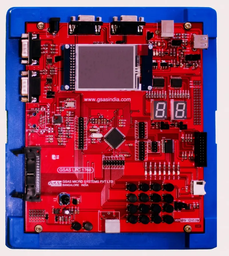
Arm Cortex-M3 evaluation board built around NXP LPC1768, on-board debugger, peripheral headers, and GSAS reference BSP. Designed and assembled in India.
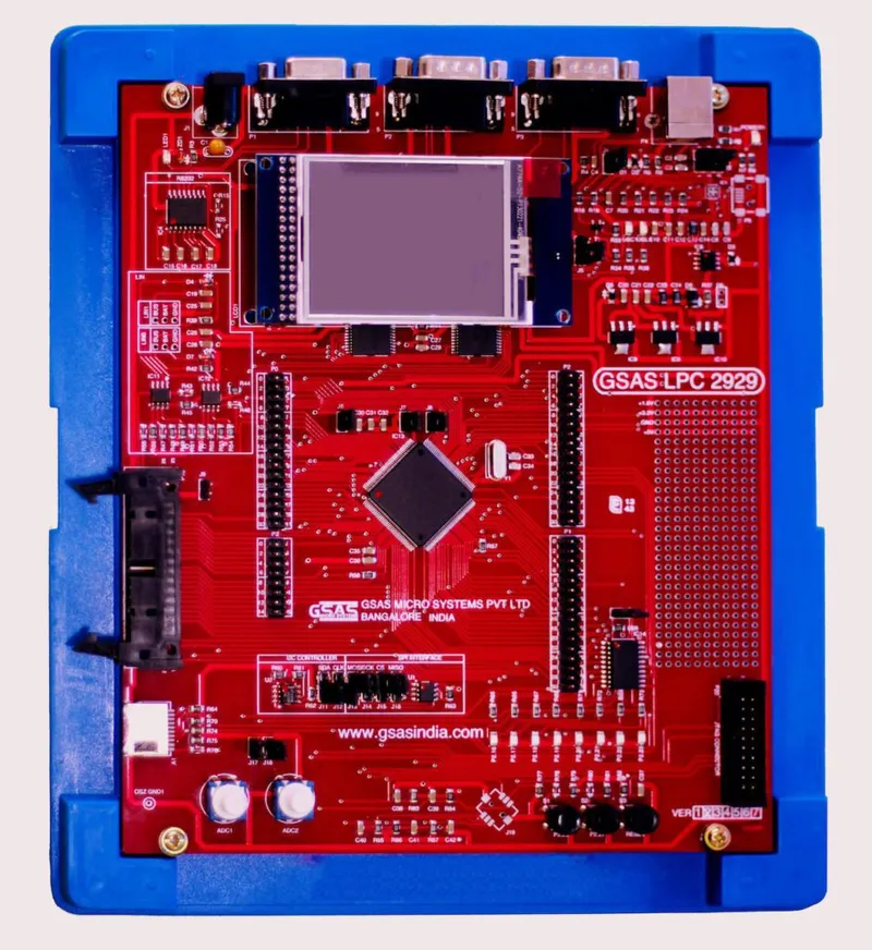
ARM9 evaluation platform built around NXP LPC2929, CAN gateway development, automotive prototyping, and embedded Linux BSP support. Available in India from GSAS with hands-on application engineering and local support.
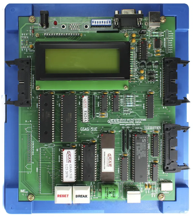
8051 microcontroller training system with peripheral ICs (8155, 8255, 8253, Keyboard Controller UPI), 20x4 LCD, and comprehensive lab manual for embedded systems education. GSAS India partner.
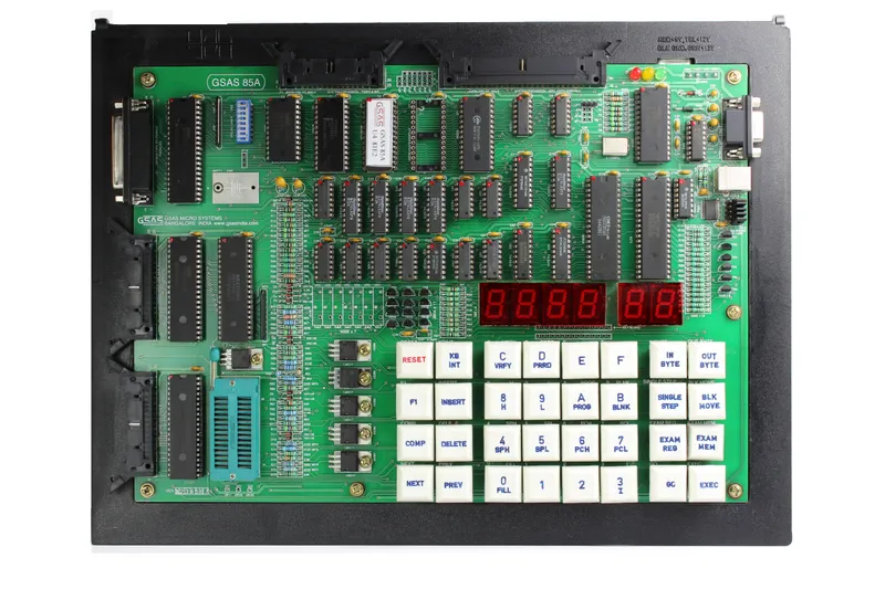
Classic 8-bit microprocessor training system based on Intel 8085, with hex keypad, LED display, built-in monitor, and expansion interface for peripheral study cards. Buy in India from GSAS.
The board is fabricated and ready, and we are demonstrating it at BIEC Bengaluru from 16 September. Pre-order the Genesis Cortex-M4 Bridge through GSAS, or talk to our Bangalore engineering team about the board, its firmware and the wider Genesis series.