Embedded Systems Companies in Bangalore: 2026 Ecosystem Guide

Inside India's densest embedded engineering cluster, the semiconductor design centres, automotive Tier-1 R&D, aerospace and defence electronics, 5G telecom, EV battery systems, and medical device teams that make Bengaluru the embedded capital of Asia.

India's embedded engineering capital didn't happen by accident

Bengaluru is the densest embedded engineering hub in Asia. Every major global semiconductor vendor, Arm, Intel, AMD, Qualcomm, NXP, Renesas, Texas Instruments, runs a design centre here. Automotive Tier-1 suppliers (Bosch, Continental, Visteon, Aptiv, Valeo) operate ECU firmware, ADAS algorithm, and motor-control teams of hundreds each. Aerospace and defence electronics firms, HAL, BEL, and private primes working on ISRO and DRDO programmes, work alongside 5G telecom R&D centres for Nokia, Ericsson, and Samsung.

But this density is not a recent accident of globalisation. It is the compounding result of a hundred years of deliberate institution-building, some of it by the Tatas, some by the Indian state, some by a single American semiconductor company that took a risk in 1985 and unknowingly set the template for everything that followed.

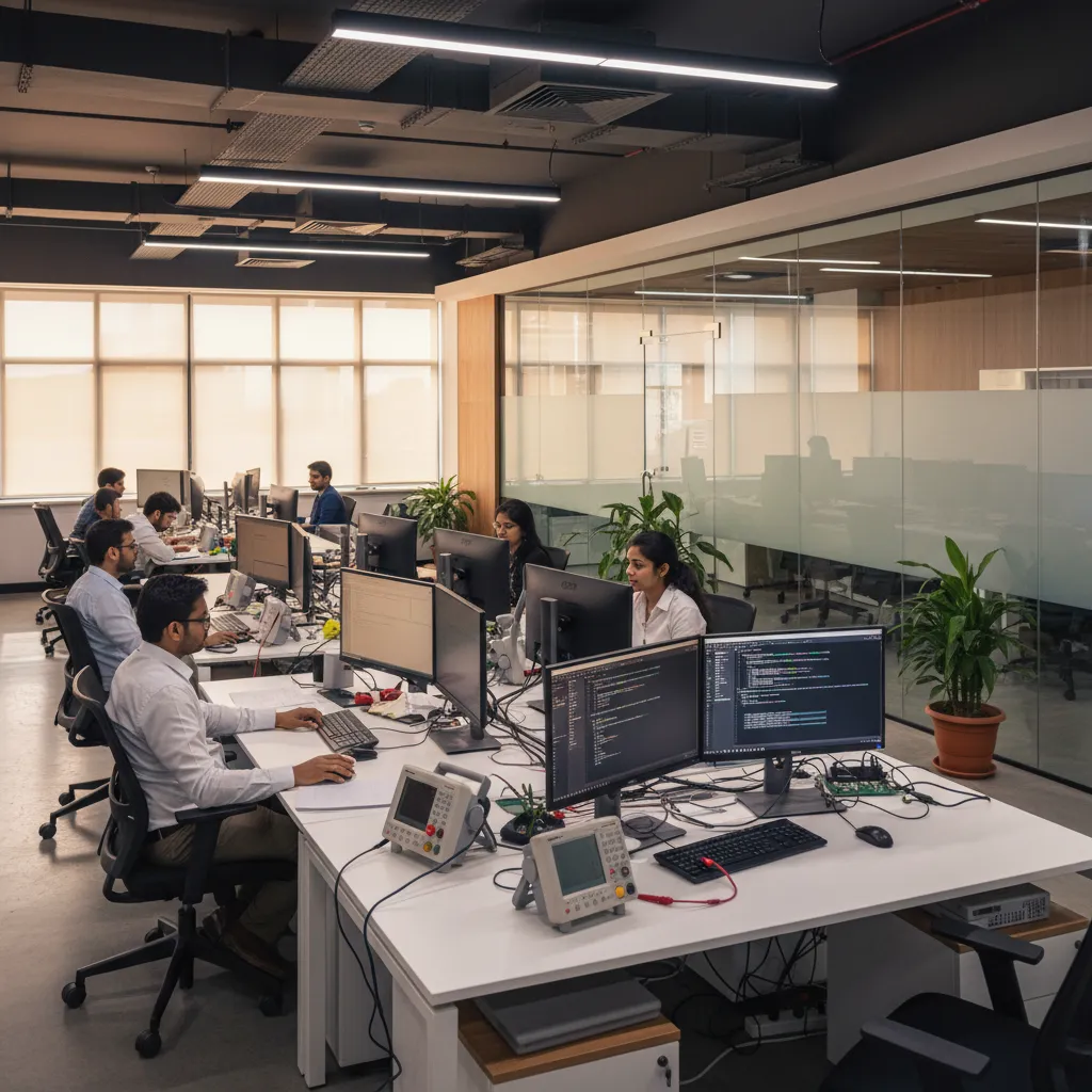
This page tells that story as the real chronology of how Bengaluru became the place where engineers get hired, where silicon gets designed, and where Indian embedded products get shipped. GSAS Micro Systems has operated inside this ecosystem as an embedded engineering partner for 14+ years. Our applications engineers came from Bengaluru's product teams before they joined us, which is why we understand the ecosystem from the inside.

From IISc to Silicon Plateau: a hundred-year arc

How one south Indian city became the design centre for a global electronics industry.

1909: The Tata moment

Jamsetji Tata plants a research university
Indian Institute of Science founded 1909: Bangalore's oldest research institution

Bengaluru's engineering story begins with a vision that predates the modern republic. In the late 1890s, the industrialist Jamsetji Tata concluded that India could never become a serious industrial power without an indigenous scientific research institution. He offered half his personal fortune to seed one, and after years of negotiation with the Maharaja of Mysore, the government of India, and a committee chaired by Nobel laureate William Ramsay, the Indian Institute of Science (IISc) was founded in Bengaluru in 1909, with land donated by the Mysore royal family on the northern edge of the city.

IISc was the first scientific research institution of its kind in Asia. Its early departments, chemistry, electrical engineering, aeronautical engineering, produced generations of Indian scientists and engineers who would later staff every major technology institution the country created. IISc is the quiet reason Bengaluru had the talent base that HAL, BEL, ISRO, C-DAC, and eventually Texas Instruments would need. Without the Tata endowment a century ago, none of what followed, none of the aerospace and defence programmes, none of the semiconductor design centres, none of the modern telecom R&D, would have had anywhere to anchor.
1940–1969: The public-sector foundation

HAL, BEL, and ISRO build the defence/space backbone

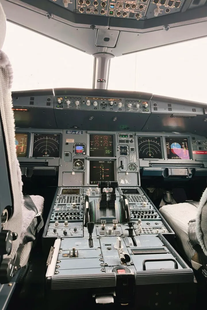
Bangalore aerospace heritage: HAL, BEL, and ISRO shaped the city's defence electronics culture

Three institutions established in Bengaluru between 1940 and 1969 built the foundation of the city's hardware-engineering culture long before the software industry arrived. Hindustan Aircraft Limited, which became Hindustan Aeronautics Limited (HAL), was established in December 1940 by Walchand Hirachand in partnership with the Mysore government, initially to assemble Harlow PC-5, Curtiss Hawk, and Vultee Vengeance aircraft during the Second World War. HAL later became the primary aerospace manufacturer for the Indian Air Force and the anchor of a domestic aerospace supply chain that today runs through GSAS customers building DO-178C avionics and MIL-STD subsystems.

Bharat Electronics Limited (BEL) followed in 1954, set up as a public-sector defence electronics manufacturer under the Ministry of Defence. BEL's Jalahalli campus in north Bengaluru became the centre of Indian radar, EW, and communication electronics manufacturing, and, more importantly for the ecosystem, a training ground for thousands of hardware engineers who would eventually populate the private sector. Many went on to ship programmes using Siemens Xpedition Enterprise for high-reliability multi-board systems and HyperLynx SI/PI for signal and power integrity sign-off.

ISRO, the Indian Space Research Organisation, was established in 1969 under Vikram Sarabhai and chose Bengaluru for its headquarters. The ISRO Satellite Centre (now U R Rao Satellite Centre), the Space Applications Centre adjuncts, and several ISRO programme offices anchored in Bengaluru, pulling satellite avionics, flight software, and ground-station engineering work into the city. ISRO's decision to headquarter in Bengaluru cemented the city as India's aerospace-electronics capital, a role it still holds today, and one GSAS supports through functional safety and compliance consulting for mission-critical programmes.

By the late 1970s, Bengaluru had a strategic mass of engineering talent, IISc graduates, HAL aerospace engineers, BEL electronics engineers, ISRO avionics engineers, concentrated in one city with a mild climate, good schools, and cultural tolerance for outsiders. All it needed was a mechanism for that talent to be turned into commercial product engineering.

1978: The first deliberate bet

Keonics builds Electronic City

Electronic City, Bangalore: India's first dedicated electronics industrial park, founded 1978

In 1978, the Karnataka government, through the state-owned Karnataka State Electronics Development Corporation (Keonics), allocated 335 acres of land 18 kilometres south of Bengaluru city centre, on the road to Hosur, specifically for electronics manufacturing and R&D companies. The area was named Electronic City and became India's first dedicated technology industrial park. In 1978 it was still a dusty periphery of the city, most of the land was scrub and farms. Today it is one of the largest IT parks in Asia, home to Infosys's global headquarters, Wipro, HCL, TCS, Biocon, Hewlett-Packard, Siemens, Tata Elxsi, and dozens of MNC R&D centres, the exact customer base GSAS engineers support with test and measurement integration, testing and validation, and hands-on training workshops every week.

Electronic City mattered because it was a deliberate infrastructure commitment. It signalled to global companies that if they wanted to open an Indian R&D office, Bengaluru would make it easy. The bet did not pay off immediately, the 1980s were a quiet decade for Electronic City, but the land was there when the wave finally arrived in 1985.

1985: The watershed year

Texas Instruments opens the first MNC R&D centre in India

Texas Instruments opened the first MNC R&D centre in India in Bangalore, 1985

In 1985, Texas Instruments, then and now one of the world's largest semiconductor companies, made a decision that would rewrite the trajectory of Indian engineering. TI opened a software design centre in Bengaluru, becoming the first multinational company to set up an R&D centre in India. The team started tiny, a handful of engineers working on DSP compiler and software tools for TI's TMS320 processor family, but the move was strategically radical.

At the time, India's foreign-exchange controls, export rules, and technology-transfer restrictions made it extraordinarily difficult for a foreign company to do serious engineering work inside the country. TI negotiated a special arrangement, used an international satellite link to connect the Bengaluru team directly to TI headquarters in Dallas, and, in a move that required dedicated government approval, became the first company in India to operate a 64 Kbps dedicated satellite link for software development. Every piece of code written in Bengaluru travelled back to Dallas over that satellite link.

TI's gamble paid off. The Bengaluru design centre grew steadily through the late 1980s, and by the mid-1990s it had become one of the company's most important global engineering sites. More importantly, TI's presence proved to every other global semiconductor and technology company that high-quality silicon engineering was possible from Bengaluru. In the years that followed, Motorola, Intel, Hewlett-Packard, IBM, Cisco, Sun Microsystems, Nortel, and dozens of others followed TI's template. The 1985 TI decision is the single most-cited milestone in every honest history of Indian technology. Today that same semiconductor design community uses Xpedition Enterprise, HyperLynx, and the broader Siemens EDA toolchain that GSAS supplies with application engineering support from our authorised partnership.

1988: The indigenous alternative

C-DAC and the PARAM supercomputer

C-DAC and the PARAM supercomputer: India's indigenous answer to export-controlled high-performance computing

Three years after TI arrived, the Indian government made an equally important bet, but in the opposite direction. In 1988, the Ministry of Electronics established the Centre for Development of Advanced Computing (C-DAC) with a specific mandate: build an indigenous supercomputer after the United States refused to export a Cray to India on strategic-technology grounds. C-DAC was set up under Dr. Vijay Bhatkar with an explicit charter and a tight deadline.

C-DAC's Pune team delivered the PARAM 8000 in 1991, India's first indigenous parallel-processing supercomputer, built around Inmos Transputer chips and benchmarked against the Cray Y-MP. PARAM 8000 was a genuine engineering achievement and a political statement: India could build its own high-end computing when shut out of imports. C-DAC went on to develop successive PARAM generations, GIST multilingual computing technology, and the BharatOS and Chitrankan OCR programmes.

C-DAC's Bengaluru centre, one of several across the country, focused on HPC systems, VLSI design tools, and embedded systems education. For decades, C-DAC Bengaluru trained thousands of Indian engineers on VLSI design methodology, FPGA verification tools, and RTL methodology, producing the talent pool that later made Bengaluru attractive to global semiconductor R&D. Many of those engineers today work in teams that rely on Questa FPGA Essentials for SystemVerilog and UVM verification and the GSAS FPGA design services that complement it. If TI's 1985 arrival was the supply side of the talent equation, C-DAC was the public-infrastructure side. Both mattered.

1991: The floodgates open

Economic reform turns a trickle into a flood

India's 1991 liberalisation triggered the MNC rush into Bangalore: Motorola, HP, IBM, Cisco all arrived

In July 1991, faced with a balance-of-payments crisis, finance minister Manmohan Singh dismantled India's licence-Raj import restrictions, opened the country to foreign direct investment, and removed most of the regulatory barriers that had made the TI arrangement exceptional. Within months, the flood began. Motorola opened a Bengaluru software design centre in 1991. Novell and Sun Microsystems followed in 1993. Hewlett-Packard opened its Bengaluru ISO Labs in 1993, initially focused on printer software. IBM returned to India in 1992 after a 15-year absence and opened a Bengaluru R&D centre shortly after. Cisco arrived in 1995.

By 1995, Bengaluru had become the default destination for any multinational technology company looking to set up an Indian R&D centre. Electronic City filled up. Whitefield, to the east of the city, began developing as a second tech corridor. Koramangala, the neighbourhood that now hosts GSAS Micro Systems among dozens of other technology firms, transformed from a quiet residential suburb into a technology cluster. The talent that IISc, HAL, BEL, ISRO, and C-DAC had spent decades producing now had dozens of global employers competing for it, and that same talent pool today fills the semiconductor design centres, automotive Tier-1 teams, and medical device startups that GSAS supports every week.

1990s–2000s: The product engineering era

From back-office work to product engineering

Silicon Plateau emerges: Intel, AMD, Nvidia, Qualcomm, Broadcom build 1000-engineer Bangalore teams

The first wave of multinational R&D in Bengaluru through the 1990s was heavy on maintenance, localisation, and back-office work, the easy, lower-risk stuff to outsource. But by the early 2000s, something shifted. Global product teams started trusting Bengaluru with front-of-product engineering work. Wireless modem firmware for Qualcomm. Graphics driver work for Nvidia. Kernel engineering for Sun Microsystems. Network-chip ASIC design for Broadcom. Baseband signal-processing algorithms for TI. That era is the reason GSAS now sells HyperLynx signal integrity into DDR5 and PCIe Gen5 design centres, and Arm Keil MDK into Cortex-M firmware teams shipping to production every week.

Infosys and Wipro, both of which had been founded earlier (1981 and 1945 respectively; Wipro pivoted from vegetable oils to IT in 1980), grew to become the largest Indian IT services firms. Wipro's Electronic City campus and Infosys's sprawling headquarters became landmarks. By the mid-2000s, Bengaluru had become the unambiguous centre of Indian technology work, not just for multinationals, but for domestic services firms exporting engineering to the world.

On the semiconductor side, the mid-2000s saw the arrival of the silicon heavyweights. Intel opened a major Bengaluru design centre. AMD built a 1000+ engineer site. Nvidia made Bengaluru its largest engineering centre outside the United States. Qualcomm built a massive modem/RF team that would eventually exceed its San Diego headcount. Broadcom, NXP (formerly Philips Semiconductors), Renesas, Infineon, and STMicroelectronics all built substantial Bengaluru teams. The city became what people now casually call the Silicon Plateau, a serious rival to Silicon Valley for semiconductor design work. These teams became heavy users of Siemens EDA tools, Arm IP and toolchains, Perforce static analysis, and the SEGGER debug ecosystem that GSAS still supplies today.

2010s–2026: The modern ecosystem

Startups, EVs, semiconductors, and the India Semiconductor Mission

Modern Bangalore engineering ecosystem: startups, EVs, semiconductors, and the India Semiconductor Mission

The 2010s saw Bengaluru layer a second ecosystem on top of the multinational R&D base: Indian technology startups. Flipkart, Ola, Swiggy, Zomato, Razorpay, Freshworks, Zoho, and hundreds of others chose Bengaluru as their headquarters. Hardware startups followed, Ather Energy for electric two-wheelers, Ola Electric, Bounce, Simple Energy, GoBee, all designing the battery management systems, motor controllers, and vehicle firmware that made Bengaluru a global EV design centre in its own right. These teams are the core customer base for GSAS's EV and energy systems solutions, combining GW Instek regenerative loads, SEGGER embOS-Safe for ISO 26262 BMS firmware, and CAN and LIN bus testing for powertrain validation.

In 2021 the India Semiconductor Mission was launched under the Ministry of Electronics and Information Technology, with a commitment of ₹76,000 crore (approximately USD 10 billion) to incentivise semiconductor and display fabrication in India. Bengaluru's existing design-centre base made the city a natural beneficiary, not for fabs directly (fabs went to Gujarat and Tamil Nadu), but for the upstream EDA, IP, and design-services ecosystem that feeds every fab. GSAS supports this ecosystem through our Siemens EDA partnership covering Xpedition, HyperLynx, Valor NPI, and Questa FPGA Essentials.

Today, Bengaluru hosts an estimated 40% of India's IT and engineering workforce, dozens of semiconductor design centres with 500-5000 engineers each, thousands of startups at varying stages, and the dense support ecosystem, IP providers, EDA tool vendors, contract design houses, EMS firms, PCB fabricators, training companies, that makes a real technology cluster work. It is a hundred years of compounding returns from the Tata endowment of 1909, and the current layer is served by capabilities like hardware design, embedded software, RTOS development, FPGA verification, and security engineering.

Where GSAS fits

A focused role inside a large ecosystem

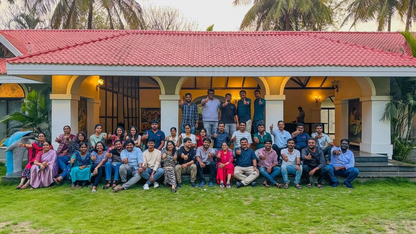
GSAS Micro Systems engineering team supporting Bangalore's product development community

GSAS Micro Systems is the authorised India engineering partner for Siemens EDA, Arm, SEGGER, Perforce, Digilent, Total Phase, GW Instek, Pico Technology, and more than a dozen other technology companies whose tools run inside Bengaluru's design centres, startups, and public-sector programmes every day.

Our applications engineers came from the Bengaluru ecosystem before joining GSAS, most have worked inside the same product teams they now support. When a design centre asks us to evaluate a HyperLynx methodology or qualify a toolchain for ISO 26262, the conversation happens between engineers who have done the work before. That is the reason GSAS has stayed relevant inside a city that tolerates no bluffing.

Six domains. One partner.

Semiconductor design in Bangalore

Semiconductor Design Centres

Bengaluru hosts one of the densest fabless semiconductor design communities in Asia. Global semi vendors run India design centres in the city, analog, mixed-signal, SoC, RF, and full-custom IC teams. These teams need EDA tools, IC layout environments, and verification methodologies that work end-to-end from RTL through tapeout sign-off.

  • Innovator3D IC layout environment (Siemens EDA), 3D IC package + silicon assembly
  • Questa FPGA Essentials for FPGA simulation and constraint-driven verification
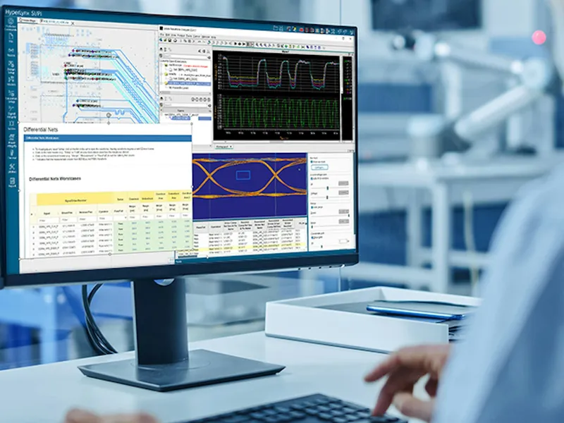
  • HyperLynx SI/PI for signal and power integrity sign-off on advanced-node SoC packages
  • Fuse EDA AI, AI-assisted design exploration for complex mixed-signal flows
Siemens EDA partnership →
Automotive ECU development in Bangalore

Automotive Tier-1 + OEM R&D

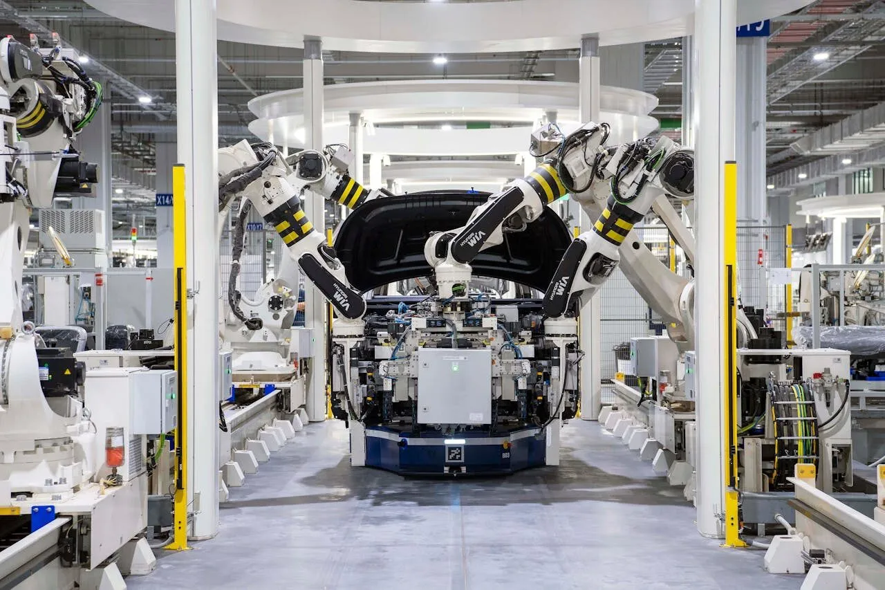
Every major global Tier-1 automotive supplier and several OEMs run ECU firmware, ADAS algorithm, and motor-control engineering out of Bengaluru. ISO 26262 compliance is table stakes, these teams need safety-qualified toolchains, MISRA C enforcement, and qualified debug/trace infrastructure for ASIL B/D programs.

  • Keil MDK v6 + Arm Compiler 6 with functional safety qualification kits
  • Klocwork + Helix QAC for MISRA C:2012 + MISRA C++:2023 enforcement
  • SEGGER embOS-Safe for IEC 61508 SIL 3 / ISO 26262 ASIL D applications
  • Razorcat Tessy for qualified unit testing + MC/DC coverage
  • DSTREAM-ST + ULINKplus trace probes for production ECU bring-up
Automotive solutions →
Aerospace electronics design in Bangalore

Aerospace, Defence, and Space

Bengaluru is India's aerospace and defence electronics hub. HAL, BEL, ISRO-adjacent contractors, and private aerospace design centres all run firmware development programs that need DO-178C and MIL-STD-compliant toolchains, radiation-tolerant design verification, and high-reliability PCB layout.

  • DO-178C tool qualification kits for Klocwork, Helix QAC, Tessy
  • Xpedition Enterprise + HyperLynx for MIL-STD high-reliability PCB design
  • IC packaging flows for radiation-tolerant FPGA + ASIC programs
  • Secure boot + TrustZone architecture consulting for defence SoCs
Aerospace & Defence solutions →
High-speed digital design in Bangalore

Telecom R&D + 5G Infrastructure

The city hosts India R&D centres for Nokia, Ericsson, Qualcomm, Intel, AMD, NXP, and several 5G infrastructure startups. These teams design high-speed digital boards with DDR5 interfaces, PCIe Gen5, 100G Ethernet, and RF front-ends that need full signal integrity sign-off before tapeout.

  • HyperLynx pre- and post-layout SI for DDR5, PCIe Gen5, USB4, 100G Ethernet
  • HyperLynx PI for power integrity sign-off on multi-rail SoC boards
  • GW Instek 3 GHz spectrum analyzers for RF pre-compliance and EMC
  • Pico Technology RF signal generators and vector network analysers
Semiconductor design solutions →
EV and battery testing in Bangalore

EV, Battery, and Energy Storage

Bengaluru's EV startup cluster, two- and four-wheeler BMS designers, motor-controller firmware teams, and charging infrastructure engineers, is one of the fastest-growing embedded segments in India. These teams need regenerative test equipment, high-voltage power supplies, and functional safety tooling for SIL-rated battery management.

  • GW Instek AEL-5000 regenerative DC electronic loads for battery discharge testing
  • GW Instek ASR AC power sources for EV charger and grid-tie validation
  • Microtest 6350 + 6632 impedance analysers for cell characterisation
  • embOS-Safe + Helix QAC for BMS firmware on ISO 26262 ASIL B/C programs
EV & Energy solutions →
Medical device development in Bangalore

Medical Device Electronics

Bengaluru medical device startups and contract design houses build patient monitors, infusion pumps, imaging front-ends, and wearables. These products need IEC 62304 software lifecycle compliance, IEC 60601 electrical safety testing, and MISRA C enforcement from day one.

  • Klocwork + Helix QAC with IEC 62304 tool qualification
  • GW Instek hipot + ground-bond safety testers for IEC 60601 compliance
  • Tessy for safety-critical unit testing with MC/DC coverage
  • SEGGER embOS for real-time firmware on patient-monitor platforms
Medical Electronics solutions →

What working with GSAS in Bengaluru looks like

GSAS is an engineering partner, not a logistics shop, our applications engineers have spent years inside the same tools we supply, and most of them came from the Bengaluru embedded ecosystem before joining GSAS. When a customer asks "how do I debug this?" or "will this toolchain qualify under ISO 26262?" or "which HyperLynx mode is right for my stackup?", the answer comes from someone who has done it on a real product.

The Bengaluru team operates out of Koramangala and covers customers across Electronic City, Whitefield, Sarjapur, Bannerghatta Road, and the northern suburbs. Demo units and evaluation licenses are available at our Bengaluru lab. On-site workshops happen regularly across customer facilities, the training team has delivered 100+ hands-on workshops on Keil MDK, Xpedition, HyperLynx, SEGGER tools, Klocwork, and Tessy across Bengaluru alone.

Procurement runs on GeM, SAP Ariba, Coupa, and TReDS platforms, we handle the invoicing infrastructure so engineering teams don't have to chase paperwork. But procurement is the least interesting part of the partnership. The interesting part is that a design team in Bengaluru can open a ticket and have an applications engineer on-site within 24 hours, reviewing their RTL, their constraints file, their trace schedule, or their qualification evidence.

Technical content from the GSAS applications team

SEGGER J-Trace and J-Link debug probes with an Andes Technology RISC-V chip, Andes Trace support announcement, available in India from GSAS
Technical Guides SEGGER

SEGGER J-Link and J-Trace Now Support Andes Trace: Why This Matters for RISC-V

SEGGER's J-Link and J-Trace probes now support Andes Trace, the hybrid N-Trace plus E-Trace instruction-trace solution built into Andes RISC-V cores. Here is what Andes Trace is, why probe-level support closes one of RISC-V's last serious tooling gaps, and what it means for Indian embedded teams.

21 Jul 2026 · 6 min read
AI data center power test bench with electronic loads and data acquisition validating a high-density rack, GW Instek instruments available in India from GSAS
Technical Guides GW Instek

AI Data Center Testing: Power Shelves, Busbars, Burn-In and Optics

AI racks fail on the bench long before they fail in the field. How AI data center infrastructure is actually tested: server power shelves and CRPS supplies, 48V busbars, battery backup units, DC-DC stages, burn-in, thermal validation, high-speed switches, and optical transceivers, mapped to the GW Instek instruments GSAS supplies across India.

20 Jul 2026 · 16 min read
Siemens EDA EBS Expert Series webinar schedule, highlighted in India by GSAS Micro Systems
Webinars Siemens EDA

Siemens EDA EBS Expert Series: 6 Free PCB Design Webinars (Jul-Aug 2026)

Siemens EDA is running six free EBS Expert Series webinars from 22 July to 27 August 2026, covering HyperLynx PI DC Drop analysis, Xpedition DRC, Xpedition EDM and PLM integration, EDX, and Starpoints/Tiebars net shorting. GSAS, the authorized Siemens EDA engineering partner in India, is highlighting all six for Indian PCB design teams.

20 Jul 2026 · 8 min read
Networked embedded test rack with debug probes for remote firmware debugging and CI/CD in India
Technical Guides SEGGER

J-Link Remote Server: Shared Debug Probes, Remote Debugging, and CI/CD Test Farms

Any USB J-Link can be shared over the network with SEGGER's free J-Link Remote Server, and the J-Link PRO puts itself on Ethernet directly. Here is how Indian firmware teams build shared labs, debug hardware across sites, and wire J-Link into CI/CD.

11 Jul 2026 · 6 min read
Setting many breakpoints in embedded flash memory during firmware debugging with a J-Link probe
Technical Guides SEGGER

Unlimited Flash Breakpoints Explained: How J-Link Does It and Which Models Include the License

Cortex-M silicon gives you 4 to 6 hardware breakpoints. SEGGER's Unlimited Flash Breakpoints removes the ceiling by reprogramming flash on the fly. Here is how the technology works, what it costs in wear and speed, and exactly which J-Link models include the license.

11 Jul 2026 · 5 min read
A hardware-free regression test run in SEGGER Ozone-Sim, set up for embedded CI/CD in India by GSAS Micro Systems
Ozone-Sim SEGGER

Hardware-Free CI/CD Regression Testing for Embedded Teams in India

Embedded regression suites are often bottlenecked by how many test boards a team owns. SEGGER's Ozone-Sim runs Arm and RISC-V firmware headless in CI, with built-in semihosting for test parameters and logged results, so regression testing no longer waits on hardware availability.

8 Jul 2026 · 4 min read

Working in Bengaluru's embedded ecosystem?

Whether you're starting a new design, qualifying a toolchain for compliance, or onboarding a team, the GSAS Bengaluru applications team is available for evaluations, demos, and on-site workshops. Response within one business day.