Product development, engineering, assembly, integration and quality testing under one roof: the manufacturing home for GSAS’s FPGA, vision AI, edge AI, automotive and production-test work.
One Building, the Whole Loop
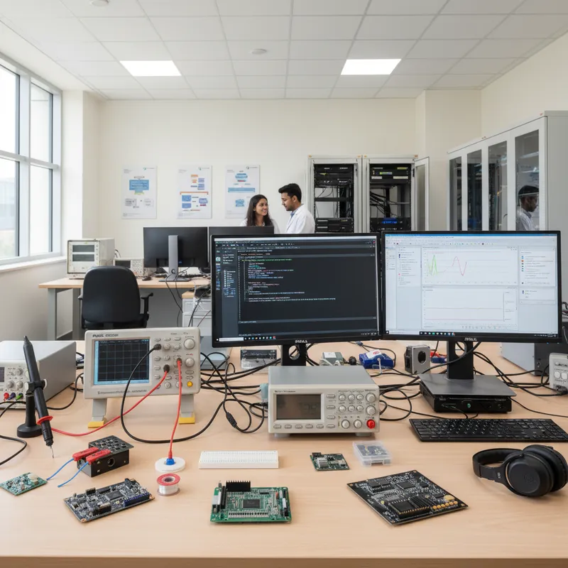
GSAS Micro Systems inaugurated its manufacturing and expanded R&D facility in Doddaballapur, Bengaluru Rural, on 5 September 2026. The building was laid out as a working environment for engineers, not a showcase: product development, engineering, manufacturing, assembly, integration and quality testing sit in the same space, so a board that fails at integration can be back on the bench of the engineer who designed it the same morning, and a change can be built and retested without leaving the site.
This page covers what that loop actually does. For the announcement itself, the ribbon-cutting and the partner and government context, see the press release.
FPGA: From RTL to a Built Board
GSAS’s FPGA design and verification work, RTL, UVM testbenches, timing closure, PS-PL integration on Xilinx and Intel platforms, now has a manufacturing counterpart in the same building. Doddaballapur is the manufacturing base for the Genesis series of GSAS-branded development boards, described in the press release as “microcontroller and FPGA development boards,” assembled and integrated on site alongside other GSAS products still in development.
The series launched on 7 September 2026 with its first board, the Genesis Cortex-M4 Bridge, an STM32F407 carrier board designed by the Bengaluru engineering team and open for pre-order. FPGA development kits are announced at the level of the series: no name, specification or ship date exists yet for a Genesis FPGA board, and when one does, it will be manufactured here.
The practical effect is that a design team working an FPGA engagement, whether through GSAS’s own services or as an authorized Siemens EDA or Digilent engagement, can move from RTL and verification into a physically built and tested board without handing the work to a separate contract manufacturer.
Vision AI and Edge AI Engineering
Anvesh Gopalam, Executive Director, described the facility’s engineering focus at the opening: “Our engineering work has been moving deeper into the FPGA space, with vision AI and edge AI projects, board bring-up support for automotive programmes, and PCBA test automation.” The edge AI and vision engineering discipline, sensor-to-inference pipelines, model optimisation, and inference on Xilinx, NVIDIA Jetson and Arm Cortex-M plus Ethos-U platforms, now has bring-up and integration bench space in the same building as the rest of the product lifecycle, rather than in a separate lab.
Automotive Board Bring-up
Board bring-up for automotive programmes, taking a new board from first power-on through validated peripherals and interfaces, is one of the facility’s stated engineering lines. It sits next to the automotive-adjacent toolchain GSAS already supplies: Arm Cortex-M and Cortex-R development tools, CAN and LIN bus testing, and automotive Ethernet validation. Bring-up work benefits directly from the one-roof layout: a board that fails a bring-up check can go back to layout or firmware the same day instead of waiting on a shipment between sites.
PCBA and Production Test Automation
The facility’s stated scope, per Anvesh Gopalam’s quote at the opening, includes PCBA (printed circuit board assembly) test automation, alongside the hardware manufacturing, assembly, integration, quality testing, R&D and new-product development that the release body describes.
The press release also states that the new site supports GSAS’s Test Solutions Integration business, government project work and ODM programmes. Anvesh Gopalam described the site as also hosting “test automation and integration work for the automotive, aerospace and satellite space.”
This is production and integration test automation on GSAS’s own build lines, not a new customer-facing service line distinct from the Test & Measurement Integration and Testing & Validation capabilities GSAS already offers. Prospective visitors can request a tour of the facility to see the test floor directly; GSAS has not published equipment lists, throughput figures or client names for this line, and none are claimed here.
A Manufacturing and Technology Support Partner for Germany and DACH
Doddaballapur is not a sales channel for partner toolchains in Germany. GSAS’s partner authorizations are territorial: the Arm and Total Phase authorizations, both exclusive to GSAS, cover India, the UAE and Sri Lanka. What Doddaballapur does support is the India-side engineering and manufacturing German and wider DACH companies need, whether that is an India entity, an Indian supplier programme, or an offshore development centre (ODC).
GSAS already supports four principals headquartered in Germany itself: ProMik of Nuremberg (partner since 2011, turnkey production flash programming and board test for tier-1 automotive suppliers), SEGGER of Monheim am Rhein (founded 1992, partner since 2025), Hitex of Karlsruhe (founded 1976, an Infineon AURIX Preferred Design House, partner since 2026) and Razorcat of Berlin (TESSY unit testing, partner since 2026). Siemens EDA, cross-linked above, is a business of Siemens AG, but its own EDA headquarters is in Wilsonville, Oregon. GSAS’s own longest India partnerships, ProT Ar-Ge and ProMik, began in 2010 and 2011, the company’s first two years, and GSAS itself was founded in Bengaluru in 2010: the honest claim is partnerships that go back to the company’s earliest years, principals with decades of their own history, and a founder, Satya Gopalam, who has worked in India’s electronics industry since the 1980s. Not decades of GSAS tenure.
The facility is the physical proof behind that pitch. Design, assembly, integration and quality testing under one roof, backed by an ISO 9001:2015 quality system and engineering support from 11 offices in nine Indian cities, is what a German parent company actually needs to evaluate before placing production or an ODC team in India: a partner whose own engineering works at the same scale, in the same toolchains, with hardware and test capability in the same building. GSAS does not hold TISAX or IATF 16949 certification and does not claim them here.
Why Germany, Specifically, Now
KPMG’s 2026 German-Indian Business Outlook survey (with the Indo-German Chamber of Commerce, AHK India) found India use as a sales market rose to 69 percent of respondents (up 18 points year on year), production base for the region to 63 percent (up 14 points), service sourcing to 55 percent (up 11 points), and shared service or global capability centres to 44 percent (up 9 points), with 80 percent of respondents planning to increase investment by 2031 and 92 percent expecting turnover growth over the same period. Every use of India in that survey rose year on year. The two that map onto the ODC pitch above, service sourcing and shared service or global capability centres, rose 11 and 9 points respectively.
Government-level movement points the same way: Germany and India signed a Joint Declaration of Intent on an India-Germany Semiconductor Ecosystem Partnership during Chancellor Friedrich Merz’s visit to India in January 2026, framed around talent, design, testing, packaging and industrial know-how rather than fab investment. Germany’s own semiconductor industry (GTAI, the federal economic development agency) reported more than EUR 17 billion in revenue in 2025 and produces more than a third of Europe’s chips, with Bavaria specifically characterised as a chip design, power electronics and automotive semiconductor hub rather than a fab region, which is the same toolchain profile Doddaballapur’s FPGA and automotive bring-up work sits in. On the automotive side, an undated VDA (German Automotive Industry Association) article whose latest referenced events are from 2022 documents German manufacturers and suppliers at more than 100 locations and production sites in India, working with ACMA and SIAM since a 2005 memorandum of understanding. German automotive buyers assess their suppliers against TISAX, the ENX Association’s information-security assessment built on the VDA ISA catalogue, which covers design data, production information, customer information, prototypes and intellectual property.
Ask for a Tour
GSAS published a walkthrough of the Doddaballapur building on LinkedIn (embedded on the press release) showing the working areas described above in use. Anvesh Gopalam’s invitation at the opening stands: “If you are curious, reach out; we are happy to give you a tour of the facility.”
Also appears in:
Need embedded development tools?
Talk to our application engineers for personalized tool recommendations.