
 Siemens EDA
 Valor NPI
DFM & ManufacturingOne manufacturing re-spin costs more than a year of Valor NPI, DFM/DFA verification with the Valor Parts Library reduces re-spins by an average of 57% per Siemens. Buy in India from GSAS.
Re-Spin Reduction
57% average (per Siemens)
Parts Library
Supply-chain-level parts data (VPL)
Input Formats
ODB++, Gerber, IPC-2581
DFM Profiles
Company, vendor, IPC, custom
Deployment
Desktop or cloud (PCBflow)
Overview
About Valor NPI
One manufacturing re-spin costs more than a year of Valor NPI. Valor NPI is Siemens EDA’s DFM and DFA verification software, proven to reduce PCB re-spins by an average of 57% (Siemens EDA, Valor NPI Fact Sheet). By shifting manufacturing knowledge left into the design process, Valor NPI identifies fabrication violations, assembly risks, yield concerns, and field reliability issues that pass standard DRC but cause real problems on the production floor. The result is faster ramp-to-volume, higher yields, and dramatically fewer costly re-spins, compressing weeks of manual DFM review into hours of automated analysis for engineering teams designing boards destined for volume manufacturing.
What Is NPI: New Product Introduction for PCB Manufacturing
New Product Introduction (NPI) is the process of taking a new electronic product from design concept through prototype validation and into volume manufacturing. NPI is where most hardware programmes succeed or fail, a single missed manufacturing constraint can force a board re-spin that costs weeks of schedule and lakhs of rupees. Traditional NPI relies on manual DFM reviews where a manufacturing engineer inspects Gerber files by eye, comparing them against fabricator capability documents. This process is slow, error-prone, and does not scale when teams are designing dense, multi-layer boards with fine-pitch BGAs and HDI microvias.
Valor NPI automates the NPI process by running the complete design, layout, components, assembly, against manufacturing rules derived from real production data. Issues are caught before Gerbers are sent to the fab house, not after prototype boards arrive with defects.
PCB Design for Manufacturability (DFM): What Valor NPI Checks
Design for Manufacturability (DFM) answers a fundamental question: can this board be fabricated correctly by my target fabricator? DFM analysis checks the bare board design against the actual process capabilities of the PCB fabrication house, minimum trace widths and spacing the fabricator can reliably etch, drill aspect ratios they can hold, annular ring sizes that survive registration tolerance, copper-to-edge clearances for routing and V-scoring, and solder mask dam widths that prevent bridging between pads.
Without DFM analysis, designers rely on generic IPC rules or the fabricator’s published capability sheets. The problem is that published specifications represent ideal conditions, real production yield depends on the interaction between multiple parameters (board thickness, layer count, material, panel size, copper weight) that generic rules cannot capture. Valor NPI’s supplier-specific DFM profiles encode the actual manufacturing constraints of your target fabricator, so analysis results reflect what your fab house can actually build, not what a datasheet says in theory.
Valor NPI applies this analysis across FR4 rigid boards, rigid-flex, flex circuits, and packaging substrates, together what Siemens EDA calls the industry’s most comprehensive DFM checks available for PCB manufacturing (Siemens EDA, Valor NPI Fact Sheet). Check weights are definable per rule, violations are flagged red, yellow, or green by severity, and every flagged item cross-probes back to its exact location in the source PCB CAD tool.
What Valor NPI Checks for Fabrication (DFM)
- Copper spacing and trace width: minimum clearances for the target copper weight and layer stackup
- Drill aspect ratio: hole depth-to-diameter ratio versus fabricator capability (critical for thick boards with small vias)
- Annular ring: pad-to-drill registration tolerance that determines whether vias survive production
- Solder mask dam width: minimum web between pads to prevent solder bridging
- Acid traps: acute-angle copper features that trap etchant and cause opens
- Copper slivers: narrow copper remnants that can detach and cause shorts
- Board edge clearance: copper and component keep-out for routing, V-scoring, and tab breakaway
- Via-in-pad: whether via-in-pad designs require filled and capped vias (additional fabrication cost)
- Impedance-critical traces: width and spacing versus stackup tolerance for controlled impedance
PCB Design for Assembly (DFA): Automated SMT Line Validation
Design for Assembly (DFA) answers the complementary question: can this board be assembled efficiently on an automated SMT line? DFA analysis evaluates component placement, orientation, solder paste deposition, reflow compatibility, and testability, everything that happens after the bare board arrives from the fabricator and enters the assembly process.
DFA issues are expensive to fix after fabrication because they often require layout changes that cascade into new Gerbers, new stencils, and potentially new bare board orders. Catching DFA violations before committing to fabrication saves both the re-spin cost and the weeks of delay.
What Valor NPI Checks for Assembly (DFA)
- Solder paste aperture violations: stencil aperture size and shape versus pad geometry, area ratio for fine-pitch components, and paste release requirements
- Component placement clearance: mechanical interference between adjacent components, pick-and-place nozzle access, and rework clearance for BGA and QFN packages
- Courtyard violations: component body and lead overlap with neighbouring parts, including 3D height conflicts
- Tombstoning risk: unequal pad sizes or unequal thermal relief on passive components (0201, 0402) that cause one end to lift during reflow
- Component orientation consistency: polarized component alignment for wave solder or selective solder processes
- Testability (ICT and flying probe): test pad placement, probe access clearance, and coverage analysis for in-circuit testing
- Thermal relief: pad connections to copper planes that affect solder joint formation during reflow
- Mixed-technology assembly: through-hole components requiring wave solder or selective solder alongside SMT components
Netlist and BOM Verification
Valor NPI’s netlist analysis compares the design’s connectivity against the expected schematic netlist, and it understands intentional shorts created by design techniques such as star points and tie bars, so these do not raise false DFM errors alongside genuine connectivity defects.
Valor NPI also verifies the bill of materials against the Approved Vendor List (BOM vs AVL), physically matching component footprints, packages, and part numbers on the BOM to what the AVL and the design database expect, catching part-substitution and footprint mismatches before they reach the assembly line.
Shift-Left DFM: Catch Manufacturing Issues Before Sending Gerbers
The traditional workflow sends Gerber files to the fabricator, who runs their own DFM check and returns a list of issues days or weeks later. Each round-trip costs schedule time. If the issues require layout changes, the designer must modify the layout, regenerate Gerbers, and restart the review cycle.
According to Siemens EDA’s Valor NPI Fact Sheet, the cost of rectifying a problem increases tenfold at each successive step of the NPI process, so a defect caught at the fabricator is far more expensive to fix than the same defect caught during layout. Valor NPI replaces this traditional iterative DFM flow with concurrent DFM: DFM rules prepared by NPI and DFM engineers are applied during design, so violations are caught while the layout is still open and inexpensive to change.
Valor NPI eliminates this cycle by running the fabricator’s manufacturing rules inside the design environment: before Gerbers are generated. The workflow is:
- Design import: Load the design via ODB++, Gerber, or IPC-2581 from any PCB tool
- Profile selection: Choose the target fabricator’s DFM profile (company-specific, vendor-specific, or IPC standard)
- Automated analysis: Valor NPI runs hundreds of fabrication and assembly checks against the manufacturing profile
- Issue review: Violations are categorised by severity (critical, warning, advisory) with precise location markers
- Design correction: Fix issues in the PCB layout tool and re-run analysis until clean
- Manufacturing handoff: Generate clean ODB++ production data with confidence that the design is manufacturable
Process-driven DFM analysis goes beyond geometry checking to evaluate designs against real manufacturing process capabilities using company-specific, vendor-specific, and IPC DFM profiles. The Valor Parts Library validates solder joints, component footprints, and assembly clearances against actual manufacturing data rather than theoretical models. Supplier DFM profiles run designs against your specific fabricator’s manufacturing rules, eliminating guesswork before prototype spin and reducing callbacks and engineering change orders during new product introduction. The Valor Parts Library (VPL) also associates each design with its correct manufacturing process and automatically selects the applicable DFM rules and values, so the right checks run without manual profile setup for every new design.
Integration with Xpedition and PADS
Valor NPI integrates directly into the Siemens EDA PCB design flow, creating a direct path from design to manufacturing verification.
With Xpedition Enterprise and Xpedition Standard: ODB++ export from Xpedition feeds directly into Valor NPI for full DFM and DFA analysis. Violations link back to the Xpedition layout, and design corrections can be made without leaving the Xpedition environment. Xpedition Standard and Enterprise subscriptions include PCBflow cloud DFM runs (see tiers below), enabling lightweight DFM checks during design without a full Valor NPI desktop installation.
With Teamcenter: Valor NPI integrates with Siemens Teamcenter for enterprise PLM workflows, linking DFM reports to design revisions and enabling manufacturing review as a formal gate in the NPI process.
PCBflow Cloud DFM Tiers
Valor NPI is available as cloud-based PCBflow or full desktop software. PCBflow cloud DFM runs are included with Siemens EDA PCB design subscriptions at different tiers:
- Essentials: 6 cloud DFM runs per year
- Standard: 12 cloud DFM runs per year
- Enterprise / Professional: Unlimited cloud DFM runs
Full desktop Valor NPI provides advanced workflows including assembly analysis, component placement verification, solder paste checks, and comprehensive panel design for teams requiring deeper DFM capabilities.
Panelization and Manufacturing Output
Optimized panel design and automation with step-and-repeat, flip-flop, and multi-design panels minimizes material waste and reduces fabrication cost. Working with any major PCB design tool through ODB++, Gerber, or IPC-2581 import, Valor NPI enables vendor-neutral DFM across Xpedition, PADS, and any major PCB design tool. Manufacturing output support includes ODB++ production data, Gerber, and IPC-2581, ensuring smooth handoff to fabrication partners worldwide.
Panel design covers fiducials, tooling holes, breakaway tabs, and v-score definition, and Valor NPI can automatically build the lowest-cost fabrication panel for a given board and order quantity, with the finished panel communicated to suppliers as manufacturing data rather than a static drawing.
Manufacturing handoff also includes the ODB++ Design package, and because ODB++ viewing is unlimited across the network, engineering, manufacturing, and supplier teams can all inspect the same handoff data without extra per-seat licensing. Design access can be shared in a controlled way through Xcelerator Share, so only the intended fabricator or partner sees the released design.
For PCB stackup design, Valor Z-planner Enterprise (the “Enterprise” here names the Z-planner product tier, not to be confused with Xpedition Enterprise) is Siemens EDA’s dedicated stackup tool, combining stackup material selection, DFM checks, and signal integrity validation in one workflow.
Valor NPI and CAM350: DFM/DFA Verification Alongside Manufacturing Data Prep
Valor NPI and CAM350 cover adjacent parts of the same manufacturing handoff. Valor NPI runs DFM and DFA verification earlier in the design cycle, against supplier-specific manufacturing profiles. CAM350 focuses on the manufacturing data itself: importing, editing, optimizing, and analyzing Gerber, ODB++, and IPC-2581 data, reverse engineering designs, and preparing panels, NC output, and test fixtures. Teams evaluating both tools from Siemens EDA can see how design-stage DFM and manufacturing data prep fit together across a PCB programme.
GSAS also highlights live Siemens EDA training relevant to PCB design and manufacturing workflows, including the EBS Expert Series webinars running July and August 2026.
Key Features
- 57% Fewer Re-Spins: Reduces PCB re-spins by an average of 57% (Siemens EDA, Valor NPI Fact Sheet). Identify fabrication and assembly issues before committing to production.
- Manufacturing DFM: Process-driven DFM analysis detects violations that pass standard DRC but impact yield, cost, or field reliability.
- Assembly DFA: Component placement, solder paste aperture, tombstoning risk, courtyard violations, and testability checks for automated assembly lines.
- Valor Parts Library: Supply-chain-level parts data. Validate solder joints, component footprints, and assembly clearances against real manufacturing data.
- Panel Design: Optimized panelization with step-and-repeat, flip-flop, and multi-design panels. Minimize material waste and reduce fabrication cost.
- Any EDA Flow: Works with any PCB tool that exports ODB++ or Gerber, Xpedition, PADS, and all major design platforms. Vendor-neutral DFM.
- Supplier DFM Profiles: Run your design against your specific fabricator’s manufacturing rules. No more guessing, know before you order.
- Cloud and Desktop: Available as cloud-based PCBflow (included with Xpedition Standard) or full desktop Valor NPI for advanced workflows.
Platform Capabilities
| Capability | Detail |
|---|---|
| Re-Spin Reduction | 57% average (per Siemens) |
| Analysis Types | Fabrication DFM, assembly DFA, solder paste, testability, panelization |
| Input Formats | ODB++, Gerber, IPC-2581, IPC-D-356 |
| Parts Library | Valor Parts Library (VPL), supply-chain-level parts data |
| DFM Profiles | Company, vendor, IPC, and custom profiles |
| Integration | Xpedition, PADS, PCBflow cloud, Teamcenter |
| DFA Checks | Solder paste, component placement, courtyard, tombstoning, ICT access |
| Output | HTML/PDF reports, ODB++ production data |
| Licensing | Desktop (FlexNet) or cloud (PCBflow subscription) |
Target Applications
- Design-for-Manufacturing: Run DFM analysis at every design milestone. Catch copper spacing, drill aspect ratio, and annular ring violations before prototype spin.
- Design-for-Assembly: Validate solder paste apertures, component placement clearance, tombstoning risk, and testability before ordering stencils and scheduling the SMT line.
- New Product Introduction: Accelerate NPI by validating designs against your contract manufacturer’s exact process capabilities. Reduce callbacks and ECOs.
- Contract Manufacturing: Fabricators use Valor NPI to analyze incoming designs, generate DFM reports, and automate data preparation for production.
- Supply Chain Resilience: Validate component footprints against manufacturing capabilities. Flag end-of-life parts and footprint mismatches before build.
Working with Indian PCB Fabricators
For hardware teams in India, DFM verification against local fabricator capabilities is essential. Indian PCB manufacturers, including AT&S India (Nanjangud), Shogini Technoarts (Gurgaon), Genus Electrotech (Mumbai), Circuit Systems India (Chennai), and Epitome Components (Bengaluru), each have specific process capabilities that differ from global fabricators in Europe, Taiwan, or China. Minimum trace widths, drill aspect ratios, via-in-pad capabilities, HDI layer counts, and impedance tolerance vary by manufacturer and by technology tier.
Running Valor NPI with a DFM profile configured for your Indian fabricator ensures that your design is validated against the specific constraints of the factory that will actually build your boards. This eliminates the common scenario where a design passes generic IPC rules but fails the fabricator’s incoming DFM check, resulting in a callback, design modification, and re-order cycle that adds weeks to the schedule.
Common DFM Issues with Indian Fabrication
- Drill aspect ratios: Some Indian fabricators have tighter limits on drill aspect ratio than global competitors, particularly for thick boards (>2.4 mm) with small vias
- HDI capabilities: Not all Indian fabricators support sequential lamination, laser-drilled microvias, or stacked via structures. Valor NPI flags these requirements before you discover them in the fabricator’s DFM report
- Impedance tolerance: Controlled impedance specifications must account for the dielectric material and manufacturing tolerance available from your specific fabricator
- Solder mask registration: Fine-pitch BGA escape routing requires tighter solder mask registration than some domestic fabricators can guarantee
From Prototype to Volume Production: Why Indian OEMs Need Valor NPI
Indian OEMs and design houses are increasingly designing complex, high-density PCBs for telecom infrastructure (5G base stations), automotive electronics (ADAS, BMS, EV chargers), defence systems (radar, EW processors), and industrial automation. The transition from prototype to volume production is where most programmes encounter manufacturing surprises, what worked as a hand-assembled prototype fails when run on automated SMT lines at scale.
Valor NPI bridges this gap by applying volume manufacturing rules during the design phase. Teams in Bengaluru, Hyderabad, Chennai, Pune, Mumbai, and Delhi NCR use Valor NPI to validate designs against their contract manufacturer’s process capabilities before committing to production tooling. The result is fewer re-spins, shorter NPI cycles, and lower total cost of product introduction, critical advantages in India’s competitive electronics manufacturing ecosystem.
Why Teams Choose Embedded DFM over Sending Gerbers to the Fab for Manual Review
Engineering teams across India are replacing the traditional Gerber-and-wait DFM workflow with embedded Valor NPI because:
- Catch manufacturing issues in design, not on the fab floor: the traditional workflow sends Gerber files to the fabricator, who returns a DFM report days or weeks later. Each round-trip costs schedule time. Valor NPI runs the fabricator’s actual manufacturing rules inside the design environment before Gerbers are even generated.
- Supplier-specific DFM profiles reflect reality: generic IPC rules represent ideal conditions. Valor NPI encodes the actual process capabilities of your target fabricator, minimum trace widths, drill aspect ratios, HDI capabilities, so analysis results reflect what your fab house can actually build, not what a datasheet says in theory.
- Design-to-manufacturing digital thread: standalone PCB tools stop at Gerber output with no insight into assembly, test, or panelization. Valor NPI validates fabrication DFM, assembly DFA, testability DFT, and panel design in a single integrated analysis, connecting design intent through manufacturing sign-off.
- The Valor Parts Library validates real solder joints: validating component footprints, solder paste apertures, and assembly clearances against actual manufacturing data. Standalone tools check only geometric spacing rules.
- 57% fewer re-spins: per Siemens EDA’s Valor NPI Fact Sheet, PCB re-spins are reduced by an average of 57%. One avoided re-spin saves more than a year of Valor NPI licensing cost.
Valor NPI vs Other DFM Analysis Tools in India
Indian hardware teams evaluating DFM analysis and design for manufacturing tools compare Valor NPI against other PCB manufacturing verification platforms. The differentiators centre on manufacturing intelligence depth, assembly verification, and integration with the design-to-production workflow.
Process-driven DFM with supplier-specific profiles: Valor NPI validates designs against the actual manufacturing capabilities of your target fabricator, not generic IPC rules. Competing DFM tools apply standardised spacing and clearance checks that represent ideal conditions. Real production yield depends on the interaction between board thickness, layer count, material, copper weight, and the specific process capabilities of your fabrication house. Supplier-specific profiles encode these constraints, so analysis results reflect what your fab can actually build.
Assembly verification (DFA) alongside fabrication DFM: Valor NPI checks solder paste apertures, component placement clearance, tombstoning risk, courtyard violations, and testability for automated SMT lines. Most competing tools focus exclusively on bare-board fabrication checks and cannot validate assembly feasibility, leaving DFA gaps that surface only when boards reach the production floor.
The Valor Parts Library validates real manufacturing data: it checks component footprints, solder joints, and assembly clearances against actual manufacturing data. Standalone DFM tools check only geometric spacing rules without part-specific manufacturing intelligence.
ODB++, Gerber, and IPC-2581 input enables vendor-neutral DFM analysis for designs from any PCB layout tool, Xpedition, PADS, or any platform that exports industry-standard formats. Teams are not locked into a single EDA vendor’s DFM workflow.
NPI automation with PCBflow cloud: cloud-based DFM runs are included with Siemens EDA PCB design subscriptions, enabling lightweight manufacturing checks during design without a full desktop installation. Full desktop Valor NPI handles advanced assembly analysis, panelization, and comprehensive manufacturing sign-off.
GSAS provides side-by-side evaluation licences so Indian teams can compare Valor NPI against their current DFM workflow on their own production designs.
Buy Valor NPI in India: GSAS India-Wide Support
GSAS provides Valor NPI with INR invoicing, local FAE support, and Siemens maintenance and support across India:
- Bengaluru: electronics OEMs and design houses validating boards against local fabricators, telecom infrastructure teams, and aerospace companies requiring first-pass manufacturing success
- Hyderabad: defence electronics organisations requiring traceable DFM sign-off for high-reliability boards, semiconductor companies, and telecom hardware manufacturers
- Chennai: automotive Tier-1 suppliers and OEMs validating ECU and BMS boards against assembly line capabilities, and PCB fabricators using Valor NPI for incoming DFM analysis
- Pune: automotive R&D centres validating DFM before prototype spin, industrial IoT companies, and contract electronics manufacturers
- Mumbai: PCB fabricators and electronics OEMs using Valor NPI for incoming design analysis, telecom infrastructure, and industrial electronics companies
- Delhi NCR: defence establishments requiring DFM traceability, telecom R&D, PCB fabricators, and automotive suppliers
- Coimbatore: industrial electronics manufacturers validating motor drive and pump controller boards against assembly line capabilities
- Visakhapatnam: naval defence electronics requiring first-pass manufacturing success, medical device companies, and industrial engineering OEMs
- Vadodara: industrial automation and power electronics manufacturers validating boards for volume production
- Kolkata: eastern India electronics manufacturers, defence electronics, and industrial engineering companies
Contact sales@gsasindia.com or call +91 80 6590 1783 for evaluation licenses, DFM profile configuration, and on-site demonstrations.
Blog
Siemens EDA Insights

India's EDA Moment: Why Design Tool Demand Is Growing, and the Engineering Careers It Creates
Electronic design automation is one of the few engineering markets where the global numbers and India's industrial policy are pointing the same direction at the same time. Here is what the published data actually says, which engineering roles the growth creates, and where GSAS Micro Systems fits as an authorized Siemens EDA engineering partner.

AI and Complexity Are Redrawing EDA: Siemens on the Trillion-Transistor Era
Siemens argues that chip complexity has outgrown siloed design and that the lines between chip, package and board can no longer be drawn. GSAS summarises the Industry Forward podcast episode and sets out what it changes for design teams in India: verify across the chip-to-board boundary before layout, not after the prototype.

Calibre Vision AI: Bringing Order to DRC Debug at Advanced Nodes
Siemens EDA's Calibre Vision AI turns full-chip DRC debug from an unmanaged flood of violations into a tracked, filtered, hand-off-able workflow. What Signal status tracking, global filters and shareable workspaces mean for Indian SoC teams.
Related products
More from Siemens EDA
All Siemens EDA products →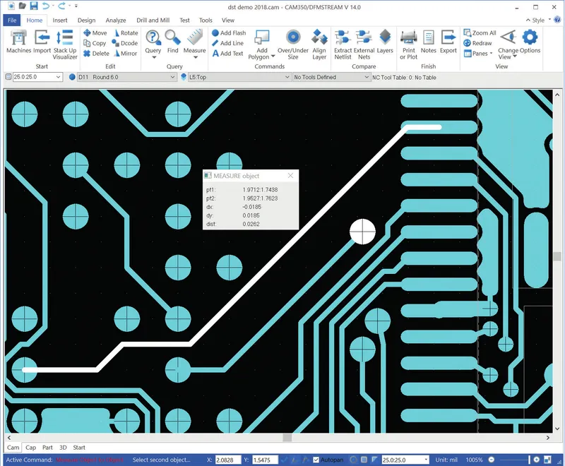
FAQ
Common questions about Valor NPI
How much does Valor NPI reduce PCB re-spins?
What file formats does Valor NPI accept?
Is Valor NPI available as cloud software or desktop only?
How much does Valor NPI cost in India?
Interested in Valor NPI?
Get pricing, an evaluation unit, or a technical consultation from our application engineers.