
Embedded Perspectives
PCB Design
37 articles tagged with PCB Design.

India's EDA Moment: Why Design Tool Demand Is Growing, and the Engineering Careers It Creates
Electronic design automation is one of the few engineering markets where the global numbers and India's industrial policy are pointing the same direction at the same time. Here is what the published data actually says, which engineering roles the growth creates, and where GSAS Micro Systems fits as an authorized Siemens EDA engineering partner.

AI and Complexity Are Redrawing EDA: Siemens on the Trillion-Transistor Era
Siemens argues that chip complexity has outgrown siloed design and that the lines between chip, package and board can no longer be drawn. GSAS summarises the Industry Forward podcast episode and sets out what it changes for design teams in India: verify across the chip-to-board boundary before layout, not after the prototype.

Siemens EDA EBS Expert Series: 6 Free PCB Design Webinars (Jul-Aug 2026)
Siemens EDA is running six free EBS Expert Series webinars from 22 July to 27 August 2026, covering HyperLynx PI DC Drop analysis, Xpedition DRC, Xpedition EDM and PLM integration, EDX, and Starpoints/Tiebars net shorting. GSAS, an authorized Siemens EDA engineering partner in India, is highlighting all six for Indian PCB design teams.
AI and Intelligent Automation in PCB Design: How Siemens Xpedition Removes the Work That Slows Indian Teams Down
Siemens' own engineers describe a 'productivity paradox' in PCB design: the tools have never been more capable, yet throughput has not kept pace. This is how AI, intelligent automation, design reuse and connected data continuity in Xpedition Standard close that gap, and what it means for PCB design teams in Bengaluru, Pune, Chennai, Hyderabad, Mumbai and Delhi NCR.

From Discovery to Production: The Modern PCB Design Journey in Siemens Xpedition: for Indian Teams
Siemens' Xpedition walkthrough 'From discovery to production' traces a single connected PCB journey, AI-assisted circuit discovery, cloud-connected tuning and simulation, AI-assisted command prediction, real-time supply-chain analysis, online design reviews, and manufacturability analysis with price estimation. Here is what that flow means for PCB design teams in Bengaluru, Pune, Chennai, Hyderabad, Mumbai and Delhi NCR, and how GSAS can share it when you ask.

ECAD-MCAD Collaboration with Xpedition for Indian Product Teams
A practical guide to ECAD-MCAD collaboration between Siemens Xpedition and NX/SOLIDWORKS/Creo for Indian product design teams, exchange formats, 3D step models, incremental change protocols, and the Indian use cases that drive adoption.
HyperLynx SI/PI: Signal and Power Integrity for Indian PCB Teams
A comprehensive guide to Siemens HyperLynx for Indian PCB teams, signal integrity, power integrity, 256-protocol compliance, electrical DRC, EM solvers, Design Space Exploration, and the Xpedition integration path.
Xpedition Standard for Indian PCB Design Teams: A Deep Dive
A comprehensive guide to Siemens Xpedition Standard for Indian PCB design teams, AI-infused sketch routing, cloud DFM via Valor, constraint management, token-based HyperLynx add-ons, and the subscription licensing path through GSAS.
Altium Designer vs Siemens Xpedition Standard: For Indian PCB Teams
A fair, technical comparison of Altium Designer and Siemens Xpedition Standard for Indian PCB design teams, schematic capture, routing, HyperLynx integration, constraint management, and the migration path from one to the other.
Flex and Rigid-Flex Design Optimization: DFM, Creepage, and Signal Integrity for Indian PCB Teams
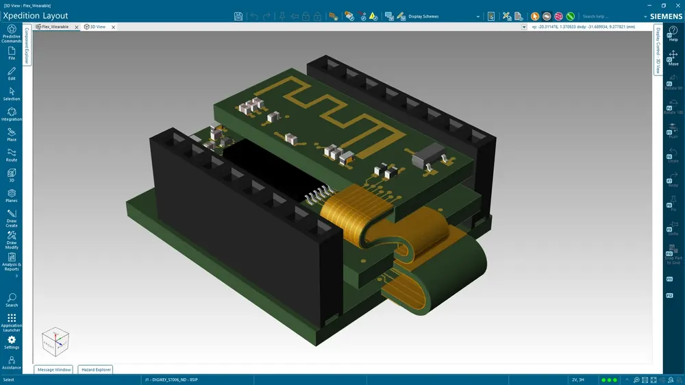
Smart and affordable DFM tools for Indian SMB teams designing flex and rigid-flex PCBs. How Siemens HyperLynx, Valor NPI, and automated creepage checking reduce NPI time and prevent expensive re-spins.
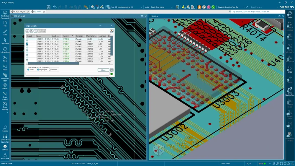
PCB Design Tool Comparison 2026: Xpedition vs Altium vs OrCAD vs PADS: An Indian Buyer's Guide
Choosing a professional PCB design tool in 2026, an honest, India-focused comparison of Siemens Xpedition Standard, Altium Designer, Cadence OrCAD, and PADS Essentials. Sourced from public OEM documentation, with a recommendation matrix by team profile.
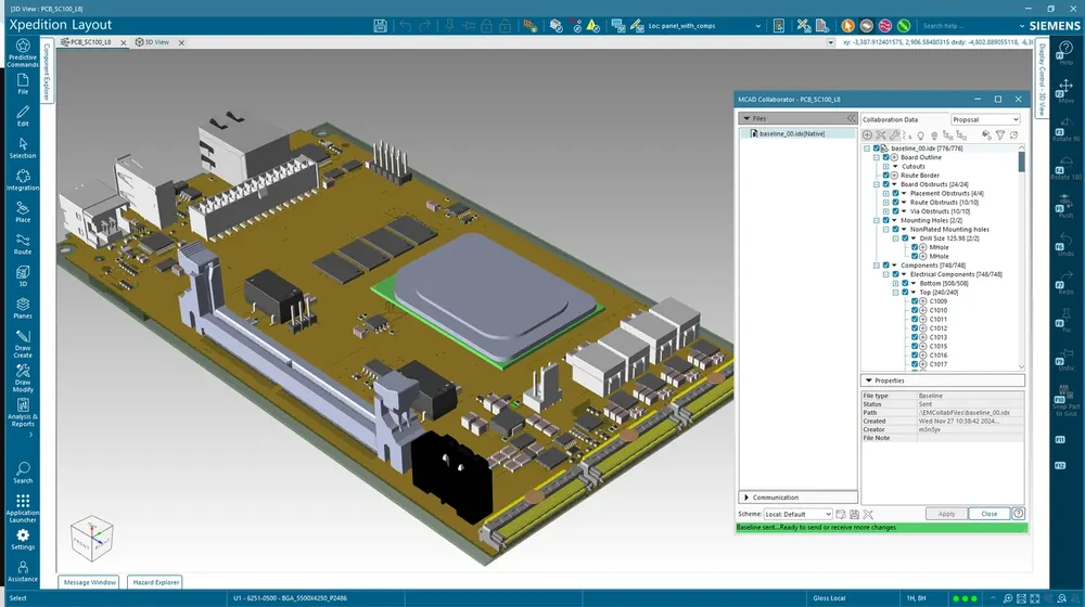
Scaling PCB Design with Adaptable Add-Ons: Signal Integrity, Rigid-Flex, and Advanced ECAD-MCAD
Watch the Siemens EDA on-demand webinar on Xpedition Standard add-ons, signal integrity, rigid-flex design, and advanced ECAD-MCAD collaboration, and see how Indian PCB design teams scale verification on demand without committing to a permanent enterprise license.
Xpedition Add-On Tokens for HyperLynx Signal Integrity: Pay-As-You-Go PCB Verification
How Siemens EDA's Xpedition token system lets Indian PCB design teams unlock HyperLynx pre-layout and post-layout signal integrity simulation on demand, without committing to a permanent SI license.
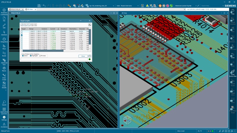
Take a Virtual Tour of Siemens Xpedition Standard: AI-Infused PCB Design
Explore Xpedition Standard through an interactive virtual tour. See the AI-infused design workflow, token-based add-ons, and why Indian engineering teams are switching from standalone PCB tools.
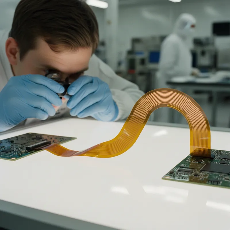
Six Challenges That Make Flex Circuits Harder to Manufacture: and How to Catch Them Before Fabrication
Flex and rigid-flex PCBs fail for reasons that standard rigid-board DFM checks completely miss: coverlay transitions, stiffener placement, copper direction at bends, and silkscreen proximity to flex zones. Here are the six challenges and how Valor NPI catches them.
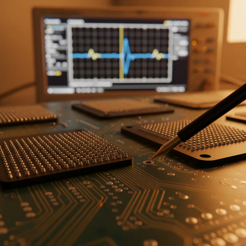
HyperLynx: Six Analysis Disciplines in One Platform: Why Fragmented Workflows Are Costing You Respins
Most PCB teams use 3-4 separate tools for SI, PI, EMI, and thermal analysis, each with its own data model and manual translation steps. HyperLynx consolidates six analysis disciplines into a single digital twin.

The PCB Designer's Triangle: Why Enterprise Verification Must Cover Reliability, Performance, and Manufacturability
Most PCB teams optimize for one corner of the design triangle and hope the others hold. Siemens EDA's integrated verification approach, HyperLynx for SI/PI, Valor for DFM, covers all three vertices in a single platform.
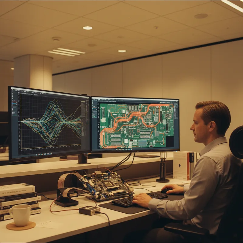
How Xpedition Add-Ons Transform PCB Design with HyperLynx Signal Integrity Analysis
Xpedition's token-based add-on architecture puts HyperLynx SI analysis within reach of every PCB designer, not just dedicated SI specialists. Pre-layout and post-layout simulation from within the layout environment, with no export steps.

Copper Thieving for PCBs: Why Manual Methods Fail and How Simulation Fixes It
Copper thieving is the standard DFM technique for improving plating uniformity, but manual thieving patterns are crude approximations. Elsyca PCBBalance automates copper balancing using electrochemical simulation, delivering uniform plating that manual methods cannot achieve.

Via Plating Reliability: Why Thin Barrels Fail and How Simulation Prevents It
Thin via barrels are the hidden reliability killer in PCB manufacturing. Elsyca PCBPlate predicts copper thickness in plated-through holes and microvias, catching thin-barrel conditions before they cause field failures.
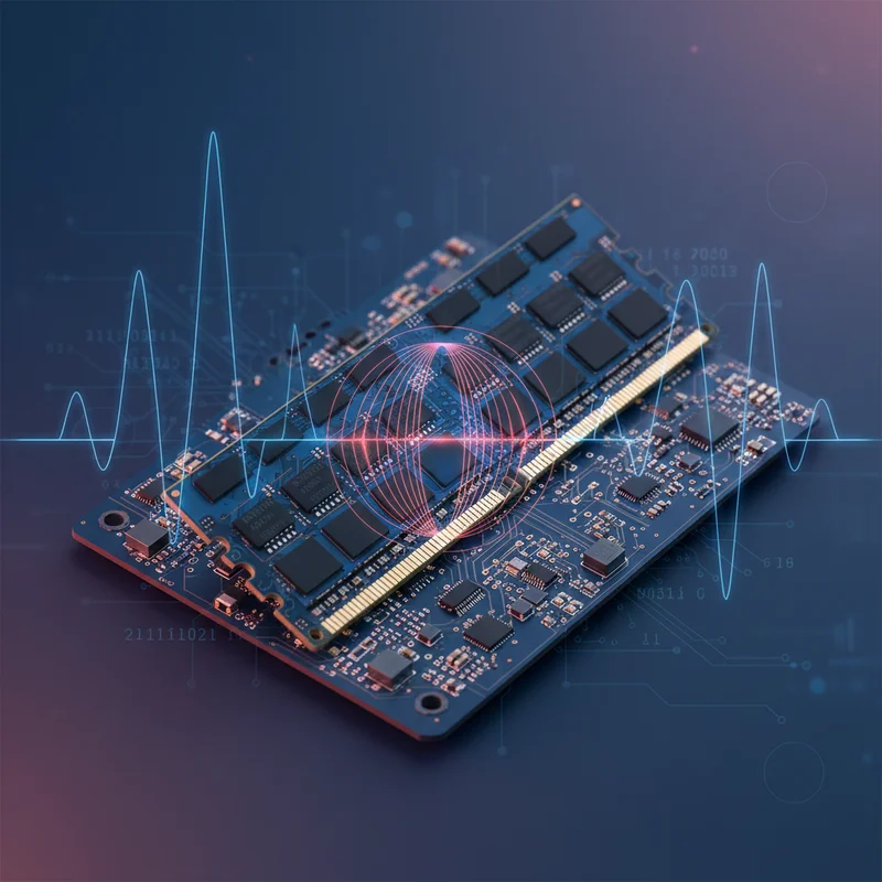
DDR5 Signal Integrity Simulation with HyperLynx: Timing, Topology, and Compliance
DDR5 at 6400 MT/s demands pre-layout topology exploration and post-layout timing validation. Learn how HyperLynx SI helps semiconductor design teams in India simulate write leveling, DQ/DQS timing, and VrefDQ noise margins.
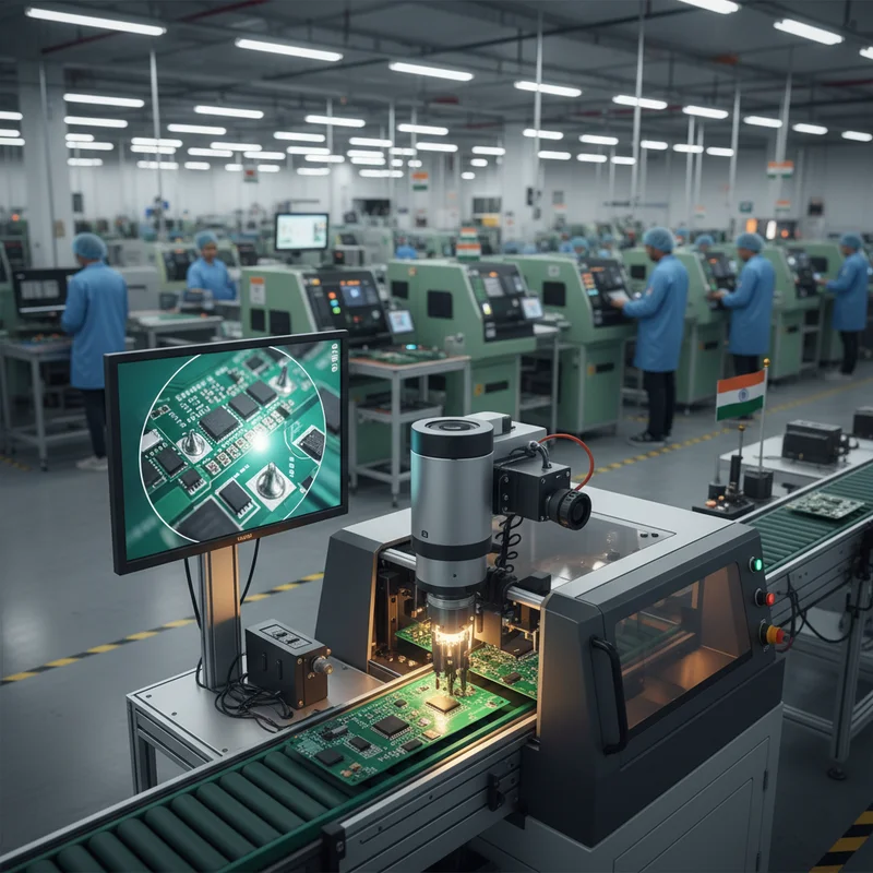
DFM and DFA for PCB Manufacturing in India: Why Your Design Needs a Manufacturability Check Before Production
Board re-spins cost lakhs and weeks of schedule. DFM and DFA analysis with Valor NPI catches solder paste violations, BGA escape failures, and fabrication constraint mismatches before your design reaches the fab house, saving Indian hardware teams from the most expensive mistake in electronics development.
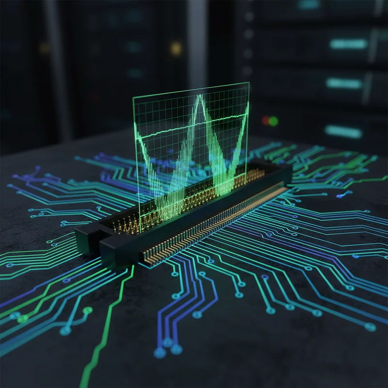
PCIe Gen5 Eye Diagram Analysis: Ensuring 32 GT/s Link Compliance in Your Design
PCIe Gen5 at 32 GT/s leaves almost no margin for channel loss. Learn how to use HyperLynx SI for eye diagram analysis, S-parameter validation, and PCI-SIG compliance checking.

Signal Integrity for High-Speed PCB Design: A Practical Guide for Indian Hardware Teams
With DDR5, PCIe Gen5, and USB4, every multi-layer PCB is now a high-speed design. Here's how Indian hardware teams can avoid common signal integrity mistakes and ship boards that work on the first spin.
Controlled Impedance and Plating Uniformity: The Connection Most PCB Designers Miss
Controlled impedance relies on trace geometry, and copper plating thickness is part of that geometry. Non-uniform plating shifts impedance outside tolerance bands. Here is how Elsyca simulation ensures your impedance targets survive the plating process.
HDI PCB Plating Challenges: Microvias, Fine Lines, and the Limits of Empirical Process Control
High-density interconnect (HDI) PCBs push electroplating to its limits, fine traces, stacked microvias, and tight impedance windows leave no margin for plating variation. Elsyca simulation tools bring predictive control to HDI manufacturing.
Plating Simulation vs DFM Rule Checks: Why Rules Alone Cannot Predict Copper Uniformity
DFM rule checks verify design constraints against fabricator capabilities. Plating simulation predicts actual copper thickness from electrochemistry. Both are needed, but they answer fundamentally different questions.
Preparing your files for Fabrication Release
When you’re done creating a new board, it’s time to send your design data to the manufacturer.
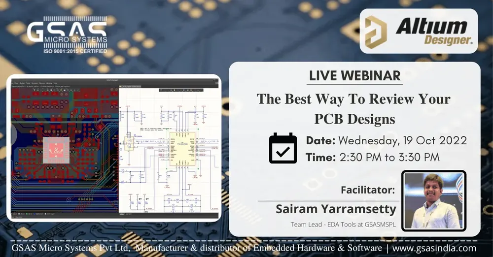
Webinar | The Best Way To Review Your PCB Designs
For many of us, building a PCB is not done by a single person.
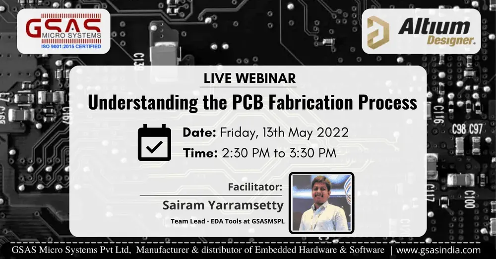
Webinar | Understanding the PCB Fabrication Process
You're done designing? Great! Now it's time to get your board fabricated. This webinar will discuss the process of getting your board fabricated, how to work with your manufacturer, and potential problems you might fa…
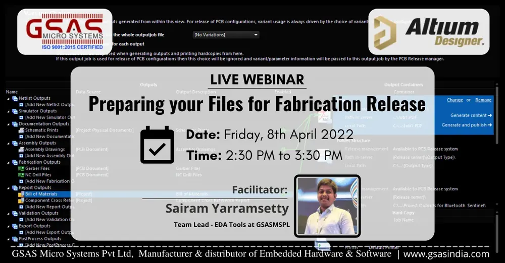
Webinar | Preparing your files for Fabrication Release
When you’re done creating a new board, it’s time to send your design data to the manufacturer. Before releasing your designs, you’ll want to make sure that everything is ready and works as intended. Join our webinar t…
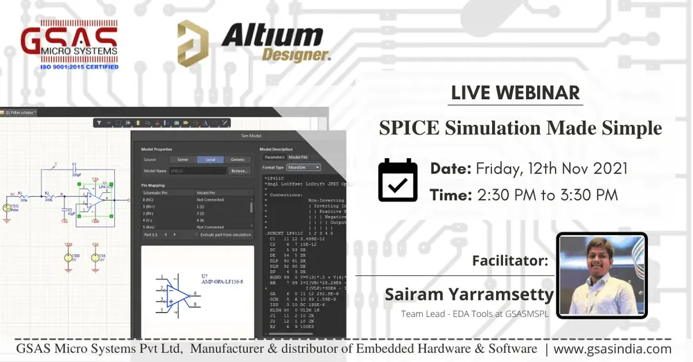
Webinar | SPICE Simulation Made Simple
SPICE simulation saves you critical time in the prototyping phase. Understanding your simulation interface makes it simple to analyze how your circuits work in different scenarios. Altium Designer provides an intuitiv…
LIVE WEBINAR II Best Practices for Successful Rigid-Flex Design
Rigid-flex PCB technology offers a tremendous amount of benefits, including reduced weight, space, increased durability, and reliability. Today’s small, lightweight mil-aero, medical, and consumer electronics products…

SPICE Simulation Made Simple
Run SPICE circuit simulations directly in Altium Designer with PSPICE and LTSPICE model support, waveform analysis, and team collaboration
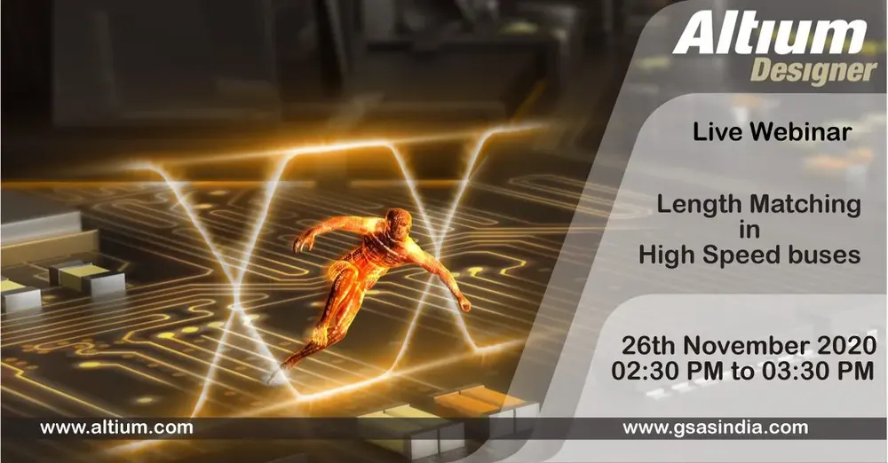
Length Matching in High Speed Buses
With ever increasing speeds in high speed data systems comes a couple of PCB layout challenges. High speed busses like DDR, VME, PCIe just to mention a few can all reach data transfer speeds that require strict timing…
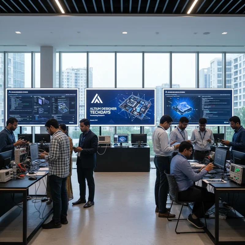
Altium Designer Techdays
A look back at Altium Designer Techday webinars and workshops hosted by GSAS, covering PCB design rules, rigid-flex, multi-board design, and more.

Understanding Design Rules and Constraints in Altium Designer
Every logical schematic design defines requirements for your physical PCB. Satisfying these requirements require understanding and consistency throughout the entire design process. How do you validate every requiremen…
Questions about PCB Design?
Our application engineers help teams evaluate tools, plan validation, and scope pilots across India.