Signal integrity analysis has traditionally been the domain of specialists, engineers with access to expensive standalone simulation tools and the expertise to operate them. For most PCB design teams in India, this has meant either skipping SI verification entirely and hoping the board works, or sending designs to an external consultant and waiting days for results. Neither approach scales.
Siemens EDA changes this equation with Xpedition’s token-based add-on architecture. Instead of purchasing a dedicated SI tool and a dedicated SI engineer, any PCB designer can invoke HyperLynx signal integrity capabilities directly within their layout environment, on demand, using tokens drawn from the same pool that powers other Xpedition add-ons. For teams in Bengaluru, Hyderabad, and Pune designing high-speed digital boards, this is a fundamental shift in how SI verification fits into the design cycle.
Pre-Layout: Catch Issues Before You Route
The pre-layout workflow starts with the stack-up editor, where designers define dielectric properties, copper weights, and layer assignments. From here, HyperLynx calculates characteristic impedances for every trace geometry and provides interactive tools for trace length optimization, terminator value tuning, and field visualization.
Key pre-layout capabilities:
- Stack-up editor: define dielectric constants, loss tangents, copper roughness, and layer spacing. Impedance targets are computed automatically.
- Terminator Wizard: sweep termination resistor values to find the optimal configuration that minimizes reflections while staying within power budget.
- Dynamic parameter sweeps: explore “what-if” scenarios: what happens if the dielectric constant shifts by 5%? If the trace width narrows at a BGA breakout?
- IBIS model assignment: assign manufacturer-provided IBIS models to drivers and receivers so simulation results reflect real component behaviour, not idealized buffers.
This pre-layout exploration happens before a single trace is routed. Issues that would otherwise surface as ringing, overshoot, or timing violations on the first prototype are caught and resolved digitally.
Post-Layout: Verify What You Actually Routed
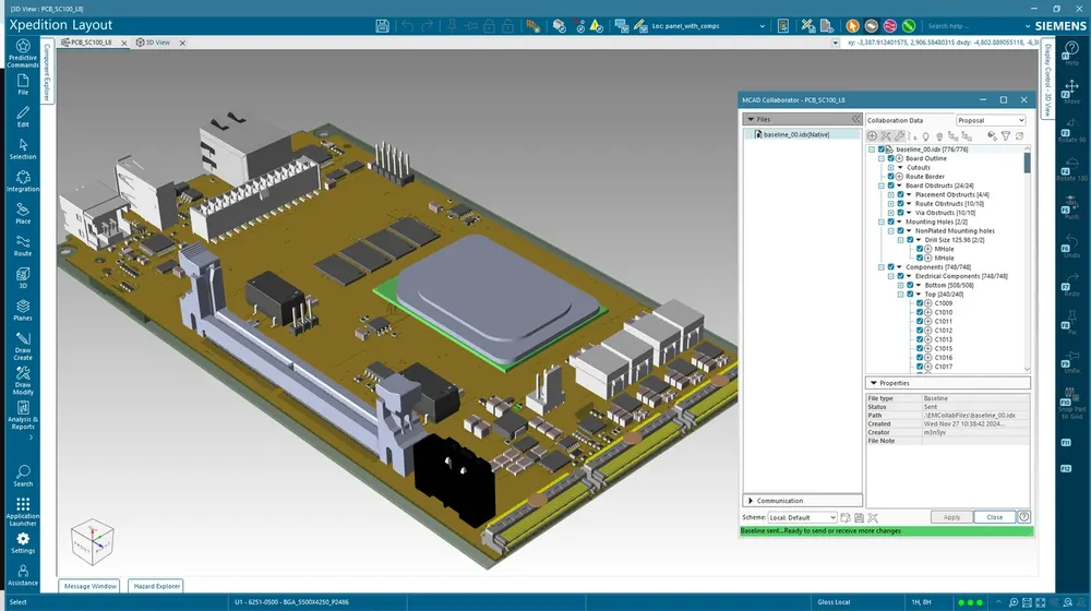
Once the board is laid out, HyperLynx launches directly from within the Xpedition layout environment. There is no export step, no file format translation, no opportunity for the simulation model to drift from the actual design.
Post-layout simulation includes:
- Net-by-net analysis: simulate individual critical nets with full topology extraction (vias, stubs, connectors, package models).
- Batch simulation: run all flagged nets in a single batch, producing an HTML report with colour-coded pass/fail results for each net against defined thresholds.
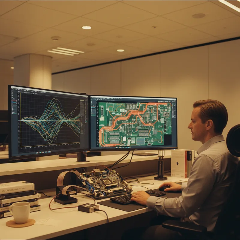
- Virtual oscilloscope: visualize waveforms at any probe point on the net, exactly as a real scope would capture them on hardware.
- Crosstalk analysis: identify aggressor-victim pairs and quantify near-end and far-end crosstalk margins.
The HTML reporting is particularly valuable for design reviews. Engineers in Chennai and Mumbai working on automotive ECU designs can generate a single SI report that covers impedance, reflection, crosstalk, and timing, then share it with the OEM as evidence of compliance.
Why This Matters for Indian Design Teams
The traditional barrier to SI analysis, cost and expertise, disproportionately affects mid-size design teams. A 5-person PCB group in Hyderabad designing a DDR4 interface doesn’t have the budget for a standalone SI tool or the headcount for a dedicated SI engineer. But they absolutely need SI verification: a single respin costs weeks of schedule and lakhs in NRE.
Xpedition’s token model solves this. The same tokens that enable advanced routing features can also enable HyperLynx SI, used only when needed, returned when done. No shelf-ware, no underutilized licenses.
GSAS Micro Systems provides Xpedition Standard and HyperLynx licensing in India with INR invoicing, token allocation guidance, and application engineering support to help teams integrate SI analysis into their existing design flow.
Also appears in:
Interested in Siemens EDA tools?
Talk to our application engineers for personalized tool recommendations.
More from Siemens EDA
View all →
India's EDA Moment: Why Design Tool Demand Is Growing, and the Engineering Careers It Creates
21 Sept · 9 min

AI and Complexity Are Redrawing EDA: Siemens on the Trillion-Transistor Era
13 Sept · 6 min

Calibre Vision AI: Bringing Order to DRC Debug at Advanced Nodes
24 Aug · 4 min

Siemens EDA EBS Expert Series: 6 Free PCB Design Webinars (Jul-Aug 2026)
20 Jul · 8 min

Emulating Processor Power for Thermal Testing: Why Constant Power
7 Oct · 7 min

CRPS and Rack Power Supply Testing: The Six Tests That Matter
7 Oct · 7 min