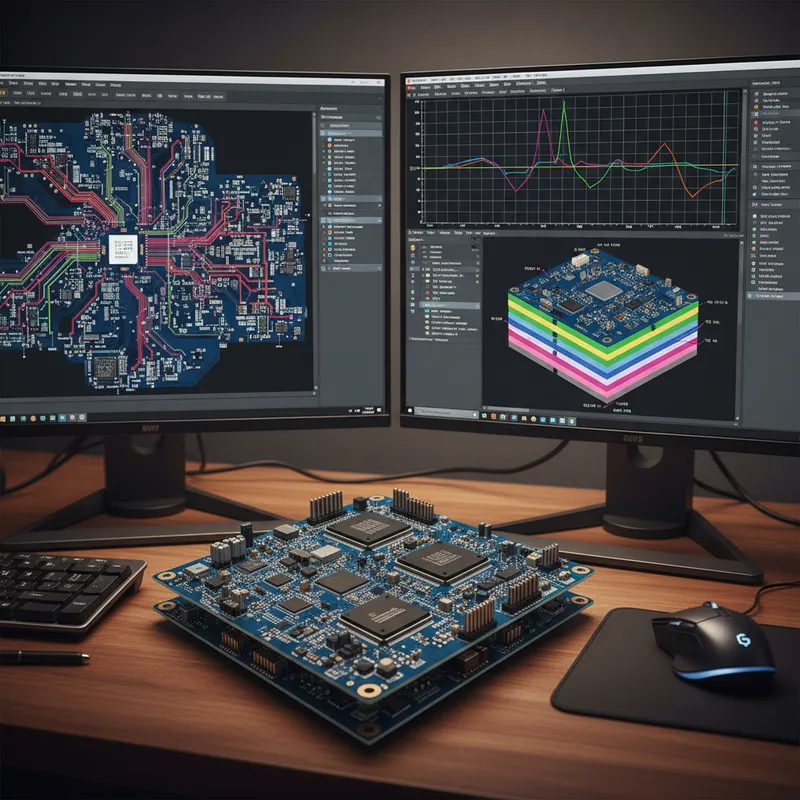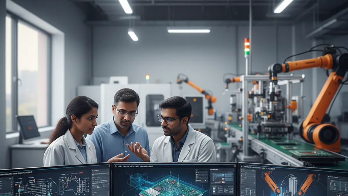
Most PCB design content treats the flow as a relay race: discovery, then design, then verification, then manufacturing, each leg handed to the next as a separate baton. The reality on a real product programme is messier, and far more interconnected. A supply-chain shortage discovered in week six sends you back to schematic capture. A signal-integrity margin found in simulation changes the placement. A manufacturability flag from the fabricator reopens the stack-up. The hand-offs are where projects actually bleed time.
Siemens’ Xpedition walkthrough “From discovery to production – a modern design journey” is built precisely to show the connected version of that journey, one continuous flow rather than four disconnected legs. It is a past, on-demand session presented by David Haboud, Senior Audience Marketing Manager at Siemens EDA, demonstrating, in Siemens’ own words, “cutting-edge PCB design techniques that streamline your journey from initial technology discovery through manufacturing release.”
This is evergreen capability content. The session itself was a scheduled webinar, but the workflow it demonstrates is exactly what the GSAS applications team can walk an Indian engineering team through on request, on your own board, with your own constraints. Below is what the journey covers, and why each stage matters for teams shipping under Indian deadlines.
The connected PCB journey, stage by stage
The session traces a single board from first idea to manufacturing-ready release, and the value is in the continuity, each stage feeds the next without a manual translation step in between. The capabilities Siemens demonstrates along the way are:
AI-assisted circuit discovery: start from intent, not a blank page
The most expensive habit in PCB design is starting at the schematic level when you should be starting at the architecture level. The journey opens with AI-assisted circuit discovery, helping the engineer move from functional intent to a candidate circuit structure quickly. For a design lead in Hyderabad weighing three sensor or power topologies, this collapses the concept phase, where the cost of indecision is highest, from days to an afternoon, while keeping the engineer as the decision-maker.
Cloud-connected circuit tuning and simulation: verify early, not at the end
Verification that waits until the end of layout is verification that arrives too late to be cheap. The session demonstrates cloud-connected circuit tuning and simulation, letting the engineer explore and validate behaviour earlier in the flow without standing up heavy local infrastructure. For Indian teams running lean, where a dedicated simulation workstation is a budget line, not a given, pulling simulation closer to the front of the design is exactly where the time saving compounds.
Efficient schematic and layout with AI-assisted command prediction
As the design moves into capture and layout, the journey shows efficient schematic and layout with AI-assisted command prediction: the tool surfacing the next likely action so the engineer spends less time navigating and more time deciding. This is the least glamorous and most immediately useful AI feature for a growing team: it shortens the ramp for new joiners from weeks to days, and it scales every time the team grows.
Real-time component supply-chain analysis
The single most disruptive thing in Indian hardware over the last few years has not been a design problem, it has been a sourcing problem. The journey includes real-time component supply-chain analysis, surfacing availability and sourcing signals while the design is still being made, when changing a part is cheap, rather than at procurement, when it is not. Catching a single-source or end-of-life part during schematic capture rather than after layout completion is the difference between a clean release and a re-spin.
Online collaboration and design reviews
Design review is where quality is either caught or missed, and distributed teams make it harder. The session demonstrates online collaboration and design reviews, so reviewers can examine the same design without a physical sign-off meeting or a stack of marked-up PDFs. For an Indian product company with a layout team in one city and stakeholders in another, or a contract house reviewing with an overseas customer, this turns review from a scheduling bottleneck into a continuous activity.
Actionable manufacturability analysis and price estimation
The journey closes where every board must: the handoff to manufacturing. The session shows actionable manufacturability analysis and price estimation, so the team understands both whether the board can be built cleanly and what it will cost before the package leaves the company. Bringing manufacturability and cost forward, into the design, rather than into a post-tape-out surprise, is the entire point of a connected flow.
Why the connected journey matters more in India
Each capability above is useful on its own. The reason the “discovery to production” framing matters is that the advantage comes from the connections between stages, not the stages themselves.
Indian product companies, contract design houses and automotive Tier-1s typically run more concurrent projects per engineer than peers in other markets. The bottleneck is rarely raw layout skill, Indian PCB engineers are among the best anywhere. The bottleneck is how many projects a senior engineer can carry without quality slipping. A connected journey, where supply-chain signals reach the engineer during design and manufacturability reaches them before release, removes exactly the kind of late-stage rework that eats that capacity.
The teams that benefit most:
- Hardware-led product companies in Bengaluru scaling from a single flagship to a portfolio, where front-loaded discovery and early simulation set the pace.
- Automotive design centres in Pune and Chennai shipping derivatives, where supply-chain and manufacturability signals during design protect the schedule.
- Reference-design and semiconductor houses in Hyderabad building boards at high cadence, where AI-assisted entry collapses the concept phase.
- Contract design houses in Mumbai and Delhi NCR reviewing with distributed and overseas stakeholders, where online design review removes a scheduling bottleneck.
Frequently asked questions
Is the “From discovery to production” webinar available to watch? It was a scheduled Siemens session and is part of Siemens’ on-demand Xpedition library. More usefully for an Indian team: GSAS can walk you through the same connected journey on your own board and constraints, which is far more relevant than a generic demo. Talk to GSAS to set that up.
What does “AI-assisted circuit discovery” actually do? It helps the engineer move from functional intent toward a candidate circuit structure early in the flow, removing the cold start of a blank schematic. The engineer stays the decision-maker. The AI removes the friction at the front of the design.
How does supply-chain analysis fit into the design tool? The journey surfaces real-time component availability and sourcing signals while the design is being made, when swapping a part is cheap, rather than at procurement, when a single-source or end-of-life part can force a re-spin.
What is the value of manufacturability analysis and price estimation inside the flow? It tells the team whether the board can be built cleanly and what it will cost before the release package leaves the company, turning the manufacturing handoff from a post-tape-out surprise into a design-time decision.
Which Siemens product does this journey run on? The session is built around Xpedition Standard. For the full product detail, see the Xpedition Standard product page.
Where GSAS comes in
GSAS Micro Systems is an authorised Siemens EDA engineering partner for India. GSAS is a value added distributor/reseller for these products. We have a dedicated FAE team ready to help you with custom built solutions matching your needs. Our applications and layout engineers have spent careers inside Xpedition, and we can walk your team through this exact discovery-to-production journey, on your own board, as part of an evaluation. We support PCB design teams across Bengaluru, Hyderabad, Chennai, Pune, Mumbai and Delhi NCR with structured onboarding, simulation and supply-chain workflow setup, design-review enablement, and manufacturability handoff with Valor and HyperLynx.
For related reading on the same flow, see:
- AI and Intelligent Automation in PCB Design with Siemens Xpedition
- Scaling PCB Design with Adaptable Add-Ons: Signal Integrity, Rigid-Flex, and Advanced ECAD-MCAD
- Xpedition Standard for Indian PCB Design Teams, A Deep Dive
- Choosing the Right Siemens EDA Tier for Your Team
The modern PCB design journey is no longer a relay of disconnected legs. It is one continuous flow from discovery to production, and the most useful thing we can do is walk an Indian engineering team through it on their own board, when they ask.
Source: Siemens EDA, “From discovery to production – a modern design journey”, presented by David Haboud, Senior Audience Marketing Manager at Siemens EDA. The capability names referenced are Siemens trademarks. GSAS Micro Systems is an authorised Siemens EDA engineering partner in India.
Also appears in:
Interested in Siemens EDA tools?
Talk to our application engineers for personalized tool recommendations.
More from Siemens EDA
View all →
India's EDA Moment: Why Design Tool Demand Is Growing, and the Engineering Careers It Creates
21 Sept · 9 min

AI and Complexity Are Redrawing EDA: Siemens on the Trillion-Transistor Era
13 Sept · 6 min

Calibre Vision AI: Bringing Order to DRC Debug at Advanced Nodes
24 Aug · 4 min

Siemens EDA EBS Expert Series: 6 Free PCB Design Webinars (Jul-Aug 2026)
20 Jul · 8 min

Emulating Processor Power for Thermal Testing: Why Constant Power
7 Oct · 7 min

CRPS and Rack Power Supply Testing: The Six Tests That Matter
7 Oct · 7 min