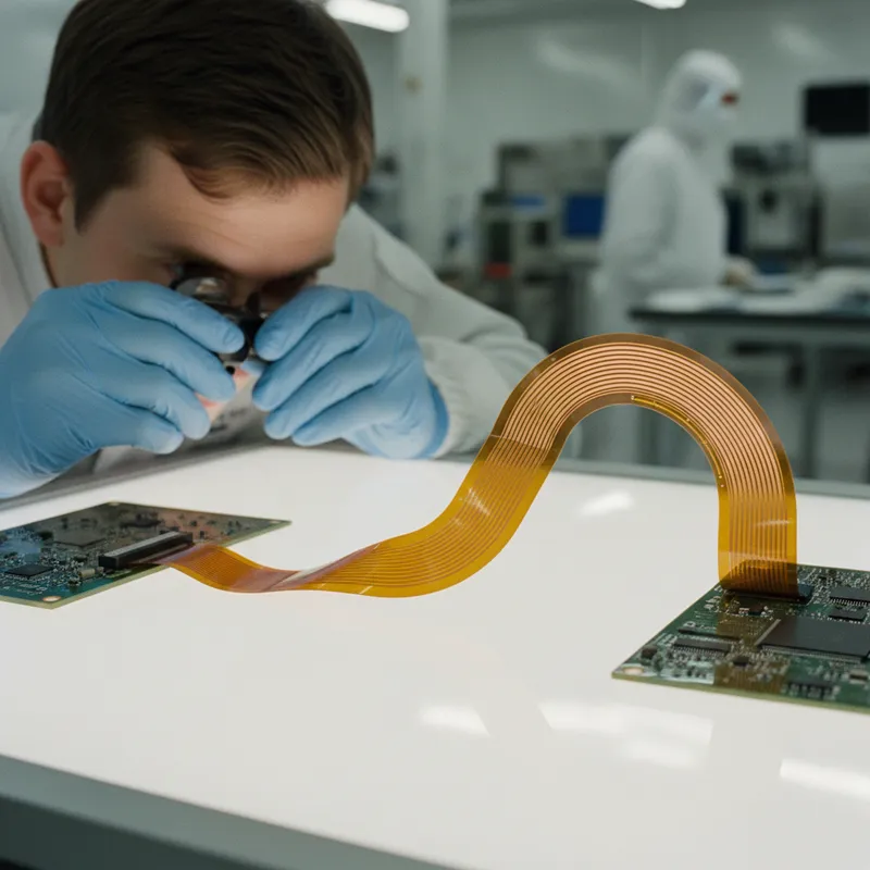
Flex and rigid-flex PCBs are fundamentally different from rigid boards, and the manufacturing challenges reflect that difference. Materials bend, coverlays are placed manually with less precision than photo-imageable solder mask, stiffeners must be located precisely to support connectors, and copper traces must follow the bend axis to avoid fatigue cracking.
Standard DFM checks designed for rigid boards miss these entirely. The result: flex circuit respins that are even more expensive than rigid board respins due to specialized tooling, longer lead times, and the limited number of fabs with flex manufacturing capability.
Here are six challenges that Indian design teams encounter when moving from rigid to flex, and how Valor NPI catches them before fabrication.
1. NSMD vs SMD Pad Definition Under Coverlays
On rigid boards, solder mask openings follow straightforward rules. On flex circuits, the interaction between coverlays and solder mask creates four distinct configurations depending on whether the pad is drilled or non-drilled and whether the mask defines or does not define the pad opening.
Mask-defined pads (SMD) provide stronger mechanical bonding, critical for connectors on flex circuits that experience repeated bending. Non-mask-defined pads (NSMD) allow solder to flow around the pad edges, improving solder joint reliability for fine-pitch components.
The wrong choice causes either weak solder joints (NSMD where SMD is needed) or bridging (SMD where NSMD is needed). Valor NPI applies context-specific rules based on the pad type, component footprint, and coverlay layer assignment.
2. Coverlay-to-LPI Solder Mask Transitions
Where the rigid section meets the flex section, the coverlay material transitions to liquid photo-imageable (LPI) solder mask. If the LPI region does not extend far enough over the coverlay edge, air gaps form, exposing copper and creating potential short circuits or corrosion paths.
This is particularly problematic in high-pitch component areas near the rigid-flex transition zone. Valor NPI checks the overlap distance and flags insufficient extension before the design reaches the fab house.
3. Stiffener Positioning and Clearance
Stiffeners are bonded to the flex circuit to provide mechanical support under connectors, ZIF sockets, and press-fit components. Incorrect stiffener positioning causes connector misalignment during assembly, solder joint damage from mechanical stress, and copper cracking at the stiffener edge.
The opposite-side coverlay must also maintain clearance from component pads, a constraint that rigid-board DFM tools do not check because rigid boards have no coverlays. Valor NPI verifies stiffener placement against both the component footprint library and the coverlay layer definition.
4. Copper Width Changes Near Bend Zones
Abrupt changes in copper trace width near stiffener edges or bend areas create stress concentration points. Under repeated flexing, these stress risers cause base material cracking and copper delamination.
The fix is to taper trace widths gradually through transition zones. Valor NPI flags any trace width change that occurs within a defined distance of a bend zone or stiffener boundary.
5. Copper Routing Direction at Bends
Traces that cross a bend zone must run parallel to the bend axis to maintain flexibility. Traces perpendicular to the bend axis resist flexing and create fatigue failure points, the copper cracks after a relatively small number of bend cycles.
This rule is counterintuitive for designers accustomed to rigid boards where routing direction is governed only by signal integrity constraints. On flex circuits, mechanical constraints override electrical preferences in bend zones. Valor NPI enforces routing direction rules relative to the defined bend axis.
6. Silkscreen Near Bend Zones
Silkscreen ink is rigid. When applied too close to a bend zone, it cracks and separates during flexing, creating debris that can cause short circuits or contamination. Valor NPI enforces a minimum clearance between silkscreen markings and defined bend zones.
The Digital Twin Approach
All six challenges share a common root cause: flex-specific manufacturing constraints that exist in physical space (coverlays, stiffeners, bend zones) but are often poorly represented in the digital design. Traditional DFM tools see only copper, mask, and drill, they do not model the mechanical layers that govern flex reliability.
Valor NPI constructs a comprehensive digital twin that maps all flex-specific layers and applies automated rules across the complete layer stack. The input format is ODB++, the same manufacturing data format used by most Indian and international fabs, ensuring that the DFM verification operates on the exact data the fab will receive.
Flex Design Support from GSAS
GSAS Micro Systems provides Valor NPI licensing, flex DFM rule configuration, and application engineering for Indian teams designing rigid-flex boards for automotive (Pune, Chennai), aerospace (Bengaluru), medical devices, and wearable electronics. Our engineers can help configure fab-specific DFM rules for your preferred flex fabricator and integrate Valor checks into your Xpedition or third-party EDA design flow.
Also appears in:
Interested in Siemens EDA tools?
Talk to our application engineers for personalized tool recommendations.
More from Siemens EDA
View all →
India's EDA Moment: Why Design Tool Demand Is Growing, and the Engineering Careers It Creates
21 Sept · 9 min

AI and Complexity Are Redrawing EDA: Siemens on the Trillion-Transistor Era
13 Sept · 6 min

Calibre Vision AI: Bringing Order to DRC Debug at Advanced Nodes
24 Aug · 4 min

Siemens EDA EBS Expert Series: 6 Free PCB Design Webinars (Jul-Aug 2026)
20 Jul · 8 min

Emulating Processor Power for Thermal Testing: Why Constant Power
7 Oct · 7 min

CRPS and Rack Power Supply Testing: The Six Tests That Matter
7 Oct · 7 min