Siemens published a piece on 10 September 2026 arguing that semiconductor complexity has moved past what traditional design methods handle, and that electronic design automation has to change shape in response. The full argument is made in an episode of the Industry Forward Podcast.
Listen to the episode
The Industry Forward Podcast, Siemens Digital Industries Software
How EDA Is Evolving for a New Era of Semiconductor Complexity
Running time 15:28. Host Dale Tutt with Ankur Gupta, Siemens EDA. Hosted by Siemens and played here from their feed, so nothing downloads until you press play.
Host Dale Tutt, Vice President of Industry Strategy at Siemens Digital Industries Software, is joined by Ankur Gupta, Executive Vice President of EDA Integrated Circuit Software at Siemens EDA, who oversees the company’s integrated circuit design portfolio.
The argument, in short
Siemens’ position is that industrial AI and rising compute demand are driving complexity faster than design methodology has kept up. In their words, “Industrial AI and growing compute demand are contributing to accelerating semiconductor complexity”, and as “transistor counts race toward one trillion per chip, the tools and workflows that engineers rely on must evolve to keep pace.”
The sharper claim is about where design boundaries sit. Gupta describes a world where “Things are interconnected at a different level” and “it’s just this massively interconnected world”. Traditional EDA, he argues, operated in “a siloed environment”, and “It’s no longer possible to draw those lines.”
What it means if you are designing in India
Strip away the scale of the numbers and the practical consequence is about where verification happens, and it applies well below the leading edge.
The silo was never a physical fact, it was a convenience. Chip, package and board were designed separately because the interactions between them were small enough to ignore, or to fix late with a respin. As speeds rise and margins shrink, those interactions stop being ignorable. A DDR5 interface is not a board problem or a silicon problem; it is both, and the failure shows up at integration.
The cost of finding it late is what changes. For a team in India shipping a product rather than a research part, the expensive event is not a complex chip. It is a prototype spin discovered to be non-functional for a reason that was visible in simulation, had anyone simulated across the boundary.
What crossing the boundary looks like on a real board. The boards our engineers are asked to look at in India tend to fail in the same place: a memory or high-speed serial interface that was routed to the reference layout, passed every physical design rule, and then would not train or would not hold its eye open in the lab. In our experience the cause is rarely inside the chip and rarely inside the board taken on its own. It sits in the transition between them, a via field under a BGA breakout, a return path that crosses a plane split, a termination scheme carried over from a different package, which is exactly the seam Gupta says can no longer be treated as a line. That is why the order of operations in HyperLynx matters more than the licence does. LineSim is the pre-layout step: the topology, driver, package and termination are simulated before a trace exists, so the choices that cause a respin are made with a waveform in front of the engineer rather than a fab drawing. BoardSim is the post-layout step: it verifies the routed board against the same protocol and DDR compliance checks and reports in the same format, so the two results can be set side by side. A team that runs only BoardSim has verified the boundary after the point at which changing it was cheap. Running LineSim first is the methodology change, and it is the larger of the two decisions; the tool purchase is the smaller one.
This is a methodology question before it is a tools question. Buying a system-level tool does not create a system-level process. The teams that benefit are the ones that change when verification happens, not just what software performs it.
The Siemens EDA tools that sit on this boundary
GSAS Micro Systems is an engineering partner for Siemens EDA, formerly Mentor Graphics, in India, and two products sit exactly where chip meets board:
- HyperLynx: signal integrity, power integrity and electrical design rule checking on one database, with LineSim for pre-layout topology exploration and BoardSim for post-layout verification. It reads Xpedition and PADS designs natively and imports any other layout tool’s design through ODB++, so the pre-layout step does not have to wait for a change of PCB tool.
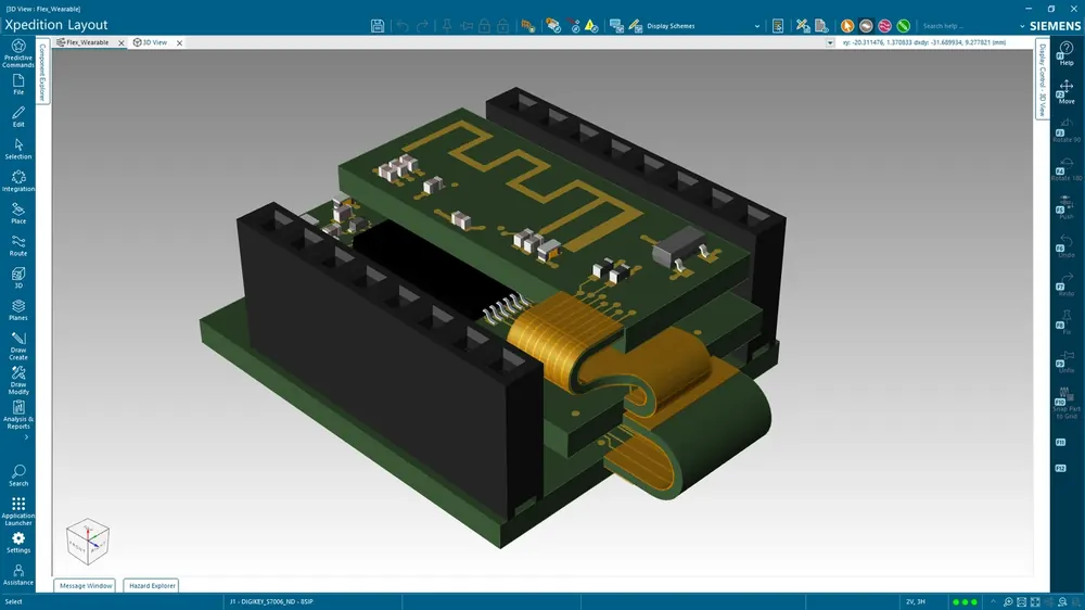
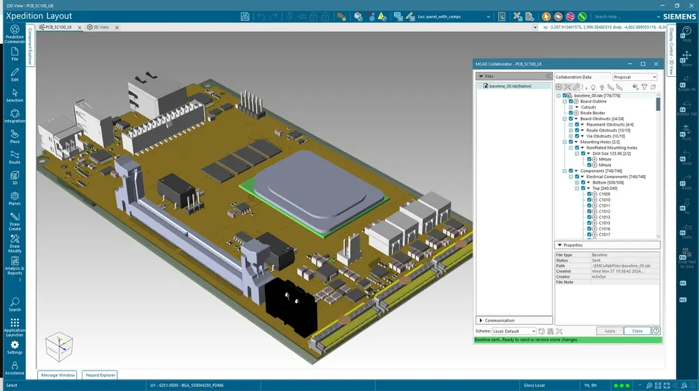
- Xpedition Standard: the PCB design flow itself, with ECAD-MCAD co-design over IDX in the base product, and HyperLynx LineSim and BoardSim available on it as token-based add-ons, so a small team can run pre-layout signal integrity from inside the design flow.
The Siemens EDA partner page carries an interactive tour of the flow and a free 30-day trial of Xpedition Standard.
GSAS engineers for Siemens EDA in India
GSAS Micro Systems is an authorized Siemens EDA engineering partner in India, with field engineers supporting design teams in Bengaluru, Hyderabad, Chennai, Pune, Mumbai and Delhi NCR. We help teams decide which verification belongs before layout, set up the LineSim-to-BoardSim flow on HyperLynx or on Xpedition Standard tokens, choose the tier a programme actually needs, and migrate a running flow without stopping work.
To talk it through, ask an engineer a question or request a quote.
Sources: Siemens Digital Industries Software, AI and complexity drive new era in EDA, 10 September 2026 and the Industry Forward Podcast episode
Also appears in:
Interested in Siemens EDA tools?
Talk to our application engineers for personalized tool recommendations.
More from Siemens EDA
View all →
India's EDA Moment: Why Design Tool Demand Is Growing, and the Engineering Careers It Creates
21 Sept · 9 min

Calibre Vision AI: Bringing Order to DRC Debug at Advanced Nodes
24 Aug · 4 min

Siemens EDA EBS Expert Series: 6 Free PCB Design Webinars (Jul-Aug 2026)
20 Jul · 8 min

AI Data Centers in India: Test, Measurement & Memory Boom
4 Jun · 14 min

Emulating Processor Power for Thermal Testing: Why Constant Power
7 Oct · 7 min

CRPS and Rack Power Supply Testing: The Six Tests That Matter
7 Oct · 7 min