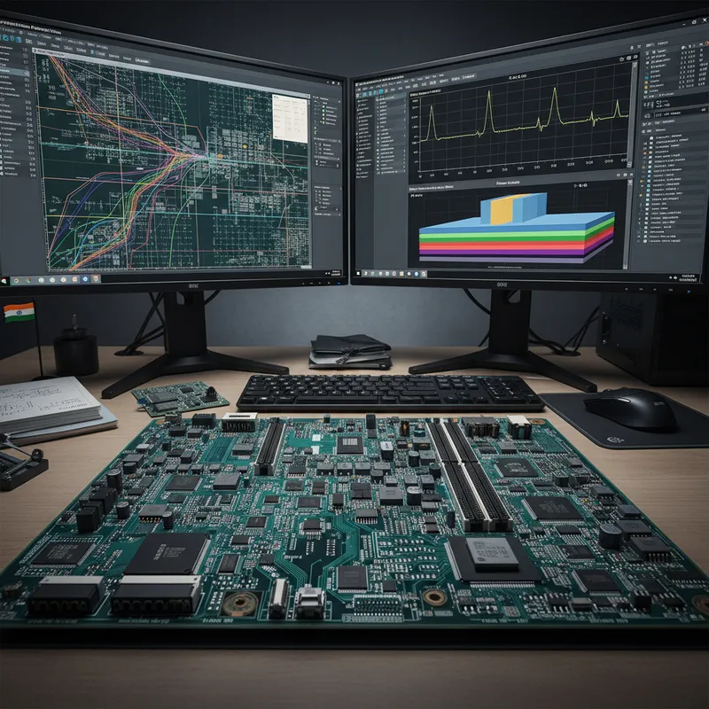
Every high-speed PCB that leaves an Indian design house carries an implicit bet: that the signal integrity margins are adequate, that the power distribution network delivers clean voltage under transient load, and that the board will pass compliance testing on the first attempt. For teams working with DDR5 at 6400 MT/s, PCIe Gen 5 at 32 GT/s, or USB4 at 40 Gbps, the margins are measured in picoseconds and millivolts. Rule-of-thumb layout practices no longer cover the gap.
HyperLynx from Siemens EDA (formerly Mentor Graphics) is the unified PCB verification platform that closes this gap. It combines signal integrity (SI), power integrity (PI), schematic analysis, electrical design-rule checking (DRC), analog mixed-signal simulation, and 3D electromagnetic solvers in a single product family, sharing one database, one stackup definition, and one simulation library. This article is the comprehensive technical guide for Indian PCB teams evaluating HyperLynx: what each module does, how they integrate, where HyperLynx fits relative to other SI/PI tools, and how to procure it with INR licensing and local engineering support through GSAS Micro Systems.
What HyperLynx Is: and What It Replaces
Most PCB design teams that perform any signal integrity work today use a patchwork of tools: a standalone SI simulator for eye diagrams, a separate PI tool for PDN analysis, a field solver for impedance extraction, maybe a SPICE simulator for analog circuits, and a manual checklist for electrical design review. Each tool has its own data model, its own stackup definition, and its own import/export friction. Every time the layout changes, the simulation setup must be updated manually, and every time it is not updated, the simulation diverges from reality.
HyperLynx replaces this fragmented workflow with a unified platform. Six verification disciplines operate on a shared representation of the PCB:
- Signal Integrity (SI): pre-layout topology exploration (LineSim) and post-layout board-level verification (BoardSim)
- Power Integrity (PI): DC IR drop, AC impedance analysis, decoupling capacitor optimization, and PDN sign-off
- Electrical DRC: extensive automated domain-based rules covering SI, PI, EMI, and electrical safety
- Schematic Analysis: automated verification against manufacturer part data to catch errors before layout begins
- Analog Mixed-Signal (AMS): SPICE + VHDL-AMS co-simulation with PCB parasitic back-annotation
- 3D EM Solvers: full-wave, hybrid, and quasi-static electromagnetic solvers in a unified framework
The practical result: an engineer who finishes a DDR5 timing analysis can immediately run a PDN impedance check on the same design, using the same stackup and the same net assignments, without exporting, translating, or re-importing anything. Changes propagate. Results cross-reference. The digital twin of the PCB stays coherent across all six domains.
Signal Integrity: LineSim and BoardSim
HyperLynx SI provides the two analysis modes that every SI workflow requires: pre-layout exploration and post-layout verification.
LineSim (pre-layout) is a schematic-level topology editor. Before a single trace is routed, the designer defines the interconnect topology, source, load, transmission line segments, termination resistors, connectors, vias, and simulates signal quality using IBIS or SPICE device models. LineSim answers the questions that must be settled before layout: maximum allowable trace length for a given data rate, termination strategy, via stub sensitivity, and crosstalk coupling at a given spacing on a given stackup.
BoardSim (post-layout) reads the routed PCB database and performs full-board SI analysis against the actual geometry, extracting real trace lengths, via transitions, plane references, and coupling paths without manual topology entry. It generates eye diagrams, bathtub curves, S-parameter matrices, and timing margin reports.
For SerDes channels, HyperLynx supports IBIS-AMI models, the industry-standard format for modeling transmitters and receivers with their equalization algorithms (CTLE, DFE, FFE). IBIS-AMI simulation produces statistical eye diagrams at the stringent bit-error-rate targets high-speed standards demand, including the JEDEC 1e-16 BER requirement for DDR5.
HyperLynx also automates channel model extraction for designs with hundreds of SerDes channels. The tool identifies which segments require 3D EM solving (BGA breakouts, via transitions, connector discontinuities) and which can use transmission-line elements, builds the end-to-end channel model automatically, and distributes EM solve jobs across available compute nodes.
Power Integrity: PDN Analysis and Decoupling Optimization
Power integrity is the discipline that Indian PCB teams most frequently skip, and most frequently pay for in re-spins. As core voltages drop to 1.0V, 0.8V, and even 0.6V for modern SoCs, the noise margin on the power rail shrinks proportionally. A PDN that delivers 3.3V with 5% ripple is adequate. A PDN that delivers 0.8V with 5% ripple has only 40 mV of margin, and a poorly placed decoupling capacitor or an inadequately sized power plane can consume that margin entirely.
HyperLynx PI addresses power integrity through four analysis capabilities:
DC IR drop analysis calculates the resistive voltage drop from VRM output to every IC power pin, accounting for copper thickness, trace width, via resistance, and current distribution. It visualizes current density to reveal hotspots and identifies pins where delivered voltage falls below the IC’s minimum supply specification.
AC impedance analysis characterizes PDN impedance (Z11) as a function of frequency and plots it against the target impedance curve, the maximum PDN impedance that keeps voltage ripple within specification. Frequency bands where the PDN fails to meet the target are highlighted immediately.
Decoupling capacitor optimization evaluates whether each capacitor is effective at its intended frequency, whether fanout routing degrades self-resonant behavior, and whether the overall strategy meets the target impedance. It recommends changes to capacitor values, quantities, and locations, reducing both component cost and board area.
Via transition analysis models impedance discontinuities and return-path disruption caused by vias passing through PDN planes, critical for designs where high-speed signals and power planes share the same stackup layers.
Indian teams designing EV battery management systems (BMS) with 0.8V core rails operating in thermal chambers at 85 degrees C find that PDN analysis is not optional. Copper resistance increases with temperature, IR drop worsens, and margins that looked adequate at 25 degrees C vanish under thermal stress. HyperLynx PI models temperature-dependent copper resistivity, allowing teams to validate PDN performance at worst-case operating temperature before committing to prototype.
Protocol Compliance: 256 Built-in Standards with Automated Pass/Fail
HyperLynx supports compliance verification for 256 built-in protocols and protocol variants. Each compliance wizard encodes the published specification’s pass/fail criteria, impedance targets, timing margins, eye mask dimensions, return loss limits, crosstalk budgets, so the designer does not need to manually interpret the specification document.
The protocols most relevant to Indian PCB teams include:
| Protocol Family | Variants Supported | Typical Indian Application |
|---|---|---|
| DDR / LPDDR | DDR3, DDR4, DDR5, LPDDR3-5 | SBC products on NXP i.MX, TI Sitara; server boards |
| PCIe | Gen 1 through Gen 5 | Defence/aerospace rugged computing, GPU backplanes |
| USB | USB 2.0, 3.x, USB4 | Medical device controllers, industrial HMIs |
| Ethernet | 1G, 2.5G, 5G, 10G, 25G, 100G | Networking equipment, automotive Ethernet TSN |
| HDMI | HDMI 1.4, 2.0, 2.1 | Display controllers, set-top boxes |
| MIPI | CSI-2, DSI, D-PHY, M-PHY | Camera interfaces for ADAS, mobile, IoT |
| JESD204 | JESD204B, JESD204C | Radar/electronic warfare ADC/DAC interfaces |
| CAN | CAN-FD | Automotive ECUs, industrial automation |
| Fibre Channel | Multiple variants | Storage area networks, data centres |
The compliance wizard workflow: select the protocol, assign the nets, run the analysis, and read the pass/fail report with margin data showing how close each parameter falls to the specification limit.
For boards with multiple protocols (a common scenario for automotive ADAS platforms with DDR5, PCIe Gen 4, Ethernet, MIPI CSI, and CAN-FD on a single ECU), batch analysis automates the process, define protocol assignments once, run all compliance checks, and generate a consolidated report.
Electrical DRC: Shift-Left Verification
HyperLynx DRC is arguably the most underappreciated module in the platform. Physical DRC, the spacing and clearance checks built into every PCB layout tool, catches geometric violations. But physical DRC cannot detect electrical issues: a signal crossing a split plane (broken return path), an antipad that clips a reference plane (impedance discontinuity), decoupling capacitors placed too far from their target IC (ineffective at the required frequency), or differential pairs with asymmetric via transitions (mode conversion).
These electrical issues cause EMC chamber failures, SI margin violations, and PDN resonances that surface only after the first prototype is fabricated. HyperLynx DRC catches them during layout, while the designer can still fix them without a re-spin.
The built-in rules are organized by domain:
- EMI rules: split-plane crossings, return-path discontinuities, clock signal routing near board edges, unshielded high-speed pairs
- SI rules: impedance violations, stub lengths, crosstalk coupling, differential pair asymmetry, via-to-pad ratios
- PI rules: decoupling placement, power-plane voiding, via antipads encroaching on power planes, copper density imbalance
- Safety rules: creepage and clearance violations for high-voltage designs (relevant to Indian EV and medical device teams)
Rules are parameterizable, the designer sets the thresholds appropriate to the design (e.g., maximum allowable stub length of 8 mils for DDR5, versus 15 mils for DDR4). Results cross-probe directly to the layout view, with ShareList integration that pans and zooms to each violation.
Python-scriptable custom rules extend the built-in rule set. Teams can encode company-specific design guidelines, “no via under BGA for QFN packages”, “minimum 3 decoupling capacitors per voltage rail”, “differential pairs must have guard traces on Layer 2”, as reusable Python scripts that run alongside the built-in checks. This captures institutional knowledge that would otherwise exist only in the heads of senior engineers.
3D EM Solvers: When Lumped Models Are Not Enough
At data rates above 10 Gbps, lumped-element transmission-line models become inaccurate for certain PCB structures. Via transitions, connector pin fields, BGA breakout regions, and package-to-board interfaces exhibit electromagnetic behavior that only a 3D field solver can capture accurately. HyperLynx provides three solver technologies within a unified framework:
Full-wave solver: maximum accuracy for via transitions at 28+ Gbps, connector S-parameter extraction, and antenna proximity analysis. Necessary for SerDes channels operating above 16 GT/s.
Hybrid solver: balances accuracy and speed for large planar structures at intermediate frequencies. Suitable for power plane impedance extraction and large via arrays.
Quasi-static solver: fast extraction for transmission-line impedance, crosstalk coupling coefficients, and analog parasitic extraction at lower frequencies.
All three solvers share the same geometry import, post-processing, and model export framework, the designer selects the appropriate solver without learning three different tools. S-parameter results feed directly into SI channel simulation, creating a continuous flow from 3D electromagnetics to system-level compliance.
Job Distribution (HL-AS JD) enables parallel execution across multiple machines, reducing wall-clock simulation time from days to hours for designs with hundreds of via transitions.
SHERPA Design Space Exploration: Automated Multi-Variable Optimization
SHERPA is the capability that separates HyperLynx from simpler SI/PI tools. Traditional SI workflow is iterative and manual: the designer adjusts one variable (trace width, via diameter, decoupling value), re-runs the simulation, evaluates the result, adjusts another variable, and repeats until the design meets specification. For a design with ten interacting variables, stackup layer thicknesses, trace widths, via geometries, termination values, decoupling capacitor values and locations, the manual approach explores a tiny fraction of the design space.
SHERPA automates this exploration. The designer defines:
- Design variables: the parameters to vary (e.g., dielectric thickness between 3.5 and 5.0 mils, trace width between 4 and 6 mils, decoupling cap value among 100 nF / 220 nF / 470 nF / 1 uF)
- Objectives: the targets to meet (e.g., characteristic impedance between 49 and 51 ohms, target impedance below 50 milliohms from DC to 1 GHz, eye height above 60 mV)
- Constraints: hard limits (e.g., total board thickness below 1.6 mm, decoupling BOM cost below a budget)
SHERPA then explores the design space, using an adaptive, surrogate-model algorithm that focuses effort on promising regions rather than sweeping every combination. The output is a set of Pareto-optimal designs representing the best achievable trade-offs among competing objectives.
For Indian teams designing constrained products, a DDR5 SOM that must fit a 1.0 mm stackup, or an automotive ECU that must meet impedance targets with a cost-optimized layer count, SHERPA finds solutions that manual iteration would miss. It transforms SI/PI optimization from an art practiced by experienced specialists into a systematic engineering process.
Integration with Xpedition, PADS, and Third-Party Tools
HyperLynx is designed to work within the Siemens EDA ecosystem, but it is not locked to it.
Xpedition Enterprise: HyperLynx integrates natively. SI/PI tools read the live Xpedition database, constraint violations propagate back to the layout editor, and design changes are immediately visible in the simulation environment. No export, no import, no version drift.
Xpedition Standard: HyperLynx capabilities are accessible through the Xpedition token system. Teams purchase a pool of tokens and consume them on demand for SI, PI, or DRC verification, making SI/PI economically accessible without a permanent standalone license.
PADS: native integration with PADS Professional and PADS Standard. HyperLynx SI, PI, and DRC run directly from the PADS environment.
Third-party PCB tools: ODB++ import lets teams using Cadence Allegro, Altium Designer, KiCad, or any other layout tool run HyperLynx verification. The integration lacks real-time back-annotation, but the analysis capabilities are identical to the native path.
This flexibility matters for Indian organizations using multiple PCB tools across product lines, HyperLynx can serve as the standardized SI/PI verification platform regardless of which layout tool each team uses.
Indian Use Cases: Where HyperLynx Solves Real Problems
Indian PCB teams encounter HyperLynx requirements across every high-speed design vertical:
DDR4/DDR5 on NXP i.MX 8/9 and TI Sitara platforms. Indian companies building Linux SBCs, industrial HMIs, and edge-AI platforms must route DDR4 or LPDDR4 interfaces with tight length-matching and impedance control. LineSim validates the topology before layout. BoardSim verifies timing margins after routing. For DDR5 on newer SoCs, simulation becomes mandatory, the timing budgets do not tolerate unvalidated routing.
PCIe Gen 4 on defence and aerospace rugged computing. VPX backplane and mezzanine interfaces require SerDes channel compliance verification. IBIS-AMI simulation confirms the channel meets the PCIe Gen 4 specification at the target BER, including connectors, via transitions, and cable assemblies.
USB 3.x on medical device controllers. HyperLynx DRC catches EMI issues that would otherwise surface during EMC chamber testing, and the USB compliance wizard validates signal quality against the USB 3.x specification.
CAN-FD on automotive ECUs. Indian automotive suppliers must validate CAN-FD bus integrity, ringing, reflections, termination adequacy, across the vehicle wiring harness. HyperLynx SI models the full topology including stubs, termination resistors, and cable lengths.
PDN analysis on EV BMS boards. Battery management systems operate with tight voltage margins on multiple low-voltage rails. HyperLynx PI’s temperature-aware DC IR drop analysis validates that rails deliver adequate voltage at worst-case operating temperature, critical for EV thermal chamber qualification.
HyperLynx vs Ansys and Cadence: Honest Trade-Offs
Indian teams evaluating SI/PI tools typically compare HyperLynx against Ansys (HFSS + SIwave) and Cadence (Sigrity). Each platform has genuine strengths. The right choice depends on the team’s workflow, design tool ecosystem, and the depth of EM analysis required.
Where HyperLynx wins:
- Design-flow integration. For Xpedition or PADS users, HyperLynx operates on the live design database with real-time back-annotation. Ansys and Cadence SI/PI tools require design export and reimport.
- Shift-left DRC. The extensive electrical DRC rules with Python extensibility have no direct equivalent in competing SI/PI workflows. Issues are caught during layout, not after fabrication.
- Six domains in one platform. SI, PI, schematic analysis, DRC, AMS, and EM solvers sharing a single database. Competing platforms typically require separate licenses with manual data translation.
- Accessibility for PCB designers. Guided workflows and protocol-aware compliance wizards, designed for layout engineers rather than dedicated EM simulation specialists.
Where Ansys and Cadence have an edge:
- Deep 3D EM for RF and package co-simulation. Ansys HFSS is the industry reference for complex RF structures, antenna arrays, and IC package co-simulation.
- IC-package-board co-analysis. Cadence Sigrity integrates deeply with Cadence IC and package design tools for chip-package-board co-simulation within the Cadence ecosystem.
The pragmatic recommendation: HyperLynx covers the SI/PI verification needs of most production PCB designs. Teams that additionally need deep RF/mmWave analysis or chip-package-board co-simulation should evaluate whether HyperLynx’s EM solvers meet their accuracy requirements for those specific use cases.
Buying HyperLynx in India: GSAS Engineering Support
GSAS Micro Systems is an authorized Siemens EDA engineering partner for India. GSAS delivers HyperLynx with INR invoicing, local field application engineering (FAE) support, training workshops, and compliance guidance for teams working in automotive (ISO 26262), defence, aerospace, and medical device domains.
What GSAS provides beyond the license:
- Evaluation licenses: hands-on evaluation on your own designs, not demo boards. Run HyperLynx SI, PI, and DRC on the actual PCB that is causing concern.
- Stackup and PDN design workshops: GSAS FAEs work with your team to define impedance-controlled stackups, validate PDN target impedance, and set up DRC rule configurations tailored to your design guidelines.
- Migration support: teams moving from other SI/PI tools to HyperLynx receive migration assistance including library conversion, workflow mapping, and training.
- Token planning for Xpedition Standard: GSAS helps teams estimate token consumption and configure the optimal token pool for their design volume and verification needs.
- Compliance guidance: support for automotive, defence, and medical device teams navigating the SI/PI verification requirements of their certification processes.
GSAS maintains engineering presence across India’s major design centres: Bengaluru (semiconductor and aerospace), Chennai (automotive and industrial), Hyderabad (defence and telecom), Pune (automotive R&D and industrial IoT), Mumbai (data-centre and fintech hardware), and Delhi NCR (defence and telecom R&D).
Contact sales@gsasindia.com or call +91 80 6590 1783 for evaluation licenses, SI/PI bundles, and on-site workshops.
Further Reading
Siemens EDA resources:
- HyperLynx product page, Siemens EDA, official product overview, datasheets, and webinar recordings
- Siemens EDA SI/PI resources, technical articles, application notes, and white papers on signal and power integrity methodology
GSAS internal resources:
- HyperLynx product page, specifications, key features, and India pricing inquiry
- Siemens EDA partner page, full Siemens EDA product portfolio available through GSAS
- Xpedition Standard, PCB design platform with token-based HyperLynx access
- Xpedition Enterprise, enterprise PCB design with native HyperLynx integration
- DDR5 Signal Integrity Simulation with HyperLynx, deep dive into DDR5-specific SI methodology
- Power Electronics PCB Design with HyperLynx, HyperLynx PI for EV and solar inverter development
- Xpedition Add-On Tokens for HyperLynx SI, pay-as-you-go SI/PI verification via the Xpedition token system
- HyperLynx: Six Analysis Disciplines in One Platform, why fragmented SI/PI workflows cost respins
- Flex and Rigid-Flex Design with HyperLynx and Valor, DFM, creepage, and SI for flex PCB designs
GSAS Micro Systems is an authorized Siemens EDA engineering partner for India, delivering HyperLynx signal integrity, power integrity, and electrical DRC solutions with local FAE support and INR invoicing across Bengaluru, Hyderabad, Chennai, Pune, Mumbai, and Delhi NCR.
Also appears in:
Interested in Siemens EDA tools?
Talk to our application engineers for personalized tool recommendations.
More from Siemens EDA
View all →
India's EDA Moment: Why Design Tool Demand Is Growing, and the Engineering Careers It Creates
21 Sept · 9 min

AI and Complexity Are Redrawing EDA: Siemens on the Trillion-Transistor Era
13 Sept · 6 min

Calibre Vision AI: Bringing Order to DRC Debug at Advanced Nodes
24 Aug · 4 min

Siemens EDA EBS Expert Series: 6 Free PCB Design Webinars (Jul-Aug 2026)
20 Jul · 8 min

Emulating Processor Power for Thermal Testing: Why Constant Power
7 Oct · 7 min

CRPS and Rack Power Supply Testing: The Six Tests That Matter
7 Oct · 7 min