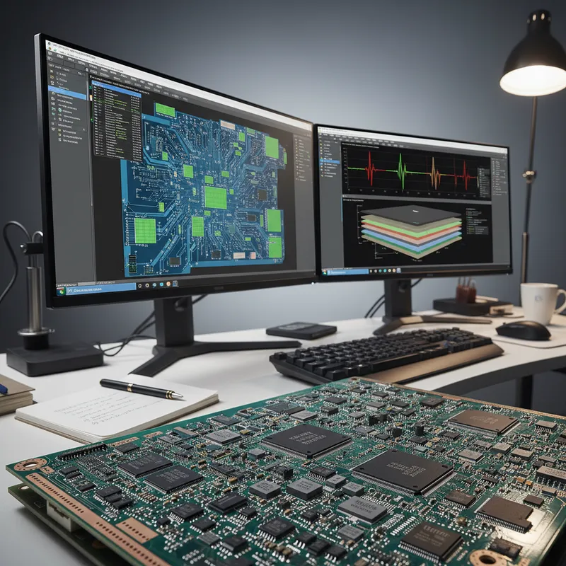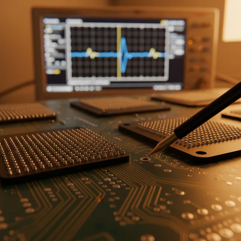
If your team uses one tool for signal integrity, another for power integrity, a third for EMI pre-compliance, and a fourth for analog simulation, you are not alone. This fragmented workflow is the norm across PCB design teams in India and globally. It is also the single largest source of unnecessary respins.
The problem is not the tools themselves. Each standalone SI or PI tool does its job. The problem is the gaps between them: manual data translation, format incompatibilities, version drift between the simulation model and the actual layout, and the sequential workflow that forces teams to complete one analysis before starting another.
HyperLynx consolidates six analysis disciplines into a single unified platform, functioning as a digital twin of the PCB that every engineer on the team can query.
The Six Disciplines
Signal Integrity (SI)
Reflection analysis, impedance matching, crosstalk quantification, and timing verification for high-speed digital interfaces. DDR4/DDR5 memory bus analysis and SerDes channel simulation (PCIe, USB, Ethernet) are core strengths. For semiconductor design teams in Bengaluru and Hyderabad building reference designs, SI verification is the first gate.
Power Integrity (PI)
DC voltage drop analysis across the power distribution network, AC impedance characterization, and decoupling capacitor optimization. HyperLynx PI identifies regions where the PDN cannot deliver clean current during transient load events, the root cause of jitter, timing margin erosion, and intermittent failures that are notoriously difficult to debug on hardware.
Schematic Analysis (SA)
Electrical rule checking at the schematic level, before layout begins. Catches connectivity errors, missing pull-ups/pull-downs, improper termination topologies, and pin assignment conflicts.
Electrical DRC
Design rule checking that goes beyond geometric DRC. HyperLynx Electrical DRC verifies high-speed routing constraints (length matching, differential pair spacing, reference plane continuity) against user-defined rules.
Analog Mixed-Signal (AMS)
SPICE-level simulation for analog circuits embedded in digital boards, op-amp stability, filter response, voltage regulator transient behaviour. For mixed-signal designs common in medical electronics (Bengaluru) and industrial instrumentation (Pune), AMS fills the gap between digital SI and full SPICE simulation.
Advanced Solvers
Three electromagnetic solver tiers:
- Quasi-Static Solver: for designs below 1 GHz where PCB structures behave as lumped elements. Fast, accurate enough for most consumer and industrial boards.
- Hybrid Solver: combines quasi-static and full-wave methods for designs in the 1-10 GHz range.
- Full-Wave Solver: rigorous 3D electromagnetic analysis for 10+ GHz designs, connector modelling, and package-level analysis.
Design Space Exploration (DSE)
The most technically ambitious feature in HyperLynx is Design Space Exploration (HL-DSE). It uses an adaptive, surrogate-model optimization algorithm to efficiently explore large design spaces, stack-up configurations, trace widths, dielectric materials, decoupling strategies, and converge on the optimal design point with a fraction of the simulations a brute-force sweep would need.
Instead of an engineer manually running 50 simulations with different stack-up parameters and eyeballing the results, DSE explores the full design space algorithmically. For teams designing high-layer-count boards (12+ layers) for automotive or telecom applications, DSE can compress weeks of iterative simulation into hours.
The Shift-Left Case
“Shift-left” means pushing verification earlier in the design cycle. When SI, PI, EMI, and DFM verification happen in parallel with layout, rather than sequentially after layout, the team catches issues when they are cheap to fix (a constraint change) rather than when they are expensive (a respin).
HyperLynx makes shift-left practical because it operates inside Xpedition. There is no export step, no model translation, no waiting for the SI engineer to finish before the PI engineer can start. Every discipline runs on the same live design data.
GSAS Support in India
GSAS Micro Systems provides HyperLynx licensing (standalone or as Xpedition add-on tokens), training, and application engineering across Bengaluru, Hyderabad, Chennai, Pune, Mumbai, and Delhi NCR. Our application engineers can help your team select the right solver tier, set up DDR/SerDes simulation templates, and integrate HyperLynx into your existing Xpedition or third-party EDA workflow.
Also appears in:
Interested in Siemens EDA tools?
Talk to our application engineers for personalized tool recommendations.
More from Siemens EDA
View all →
India's EDA Moment: Why Design Tool Demand Is Growing, and the Engineering Careers It Creates
21 Sept · 9 min

AI and Complexity Are Redrawing EDA: Siemens on the Trillion-Transistor Era
13 Sept · 6 min

Calibre Vision AI: Bringing Order to DRC Debug at Advanced Nodes
24 Aug · 4 min

Siemens EDA EBS Expert Series: 6 Free PCB Design Webinars (Jul-Aug 2026)
20 Jul · 8 min

Emulating Processor Power for Thermal Testing: Why Constant Power
7 Oct · 7 min

CRPS and Rack Power Supply Testing: The Six Tests That Matter
7 Oct · 7 min