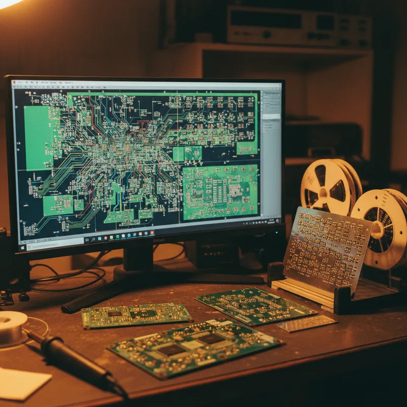
Controlled-impedance PCB design is a discipline that most high-speed design engineers understand well. Trace width, dielectric thickness, copper thickness, and dielectric constant determine the characteristic impedance of a transmission line. Signal integrity tools like HyperLynx compute the required trace geometry for target impedance values, 50 ohms single-ended, 100 ohms differential, and the designer routes traces at those widths with precise stackup control.
What many designers overlook is that the copper thickness in the impedance calculation is not the nominal foil thickness, it is the final copper thickness after plating. And plating is not uniform. The same trace can be 30 micrometres thick at one end of the panel and 40 micrometres thick at the other, depending on its position relative to the anodes and surrounding copper features. This 10-micrometre variation changes the trace cross-section geometry and shifts the impedance.
How Plating Variation Affects Impedance
The characteristic impedance of a microstrip or stripline is a function of the trace width (w), copper thickness (t), dielectric thickness (h), and dielectric constant (Er). For a typical inner-layer stripline at 50 ohms:
- A 5-micrometre increase in copper thickness reduces impedance by approximately 1-2 ohms
- A 10-micrometre increase reduces impedance by approximately 2-4 ohms
For designs with tight impedance tolerance bands (50 ohms +/- 5%), a 10-micrometre plating variation can consume half the available tolerance budget, before accounting for dielectric thickness variation, etch factor, and other manufacturing variables.
The problem compounds for differential pairs, where impedance depends on both the individual trace dimensions and the coupling between traces. Plating variation that affects both traces equally shifts the differential impedance. Plating variation that affects one trace more than the other (possible if the traces are in different current density regions) creates an impedance imbalance between the positive and negative traces.
Where Plating Variation Is Worst
Not all regions of a PCB panel experience the same plating variation. The electrochemistry creates predictable patterns:
Panel edges vs centres. Edge traces plate 30-50% thicker than centre traces in a typical vertical plating cell. A controlled-impedance trace near the panel edge may be 38 micrometres while the same trace near the panel centre is 28 micrometres.
Near pours vs isolated. Traces adjacent to large copper pours compete for plating current with the pour. The pour, with its large surface area, draws current away from the narrow trace, resulting in thinner copper on the trace. The impedance shifts upward (thinner copper = higher impedance for striplines).
Near vias. Regions with many plated-through vias draw current vertically through the panel, locally reducing the current available for surface trace plating.
The Simulation Solution
Elsyca PCBBalance and PCBPlate address the plating variation that compromises impedance control:
PCBBalance equalises the copper density across each layer, reducing the gross variation in current distribution that causes thick-edge/thin-centre patterns. By adding simulation-optimised copper thieving, PCBBalance narrows the plating thickness window across the panel.
PCBPlate provides the quantitative prediction, the actual copper thickness at each controlled-impedance trace location. The designer or fabricator can then:
- Verify that plating variation stays within the impedance tolerance budget
- Adjust trace widths to pre-compensate for predicted plating variation (wider traces in thick-plating regions, narrower in thin regions)
- Optimise panel layout to place impedance-critical traces in regions of uniform plating
This simulation-informed approach is more effective than the traditional method of adding impedance test coupons to the panel border and hoping that the coupon measurement represents the actual trace conditions across the board.
Integration with Signal Integrity Workflow
For Indian design teams using Siemens EDA tools (Xpedition, HyperLynx) for signal integrity analysis, the Elsyca plating simulation adds the manufacturing dimension that SI tools assume is constant. The workflow:
- HyperLynx determines required trace geometry for target impedance
- PCBBalance optimises copper balance for uniform plating
- PCBPlate predicts actual copper thickness at impedance-critical locations
- HyperLynx re-evaluates impedance with predicted (not nominal) copper thickness
This closed-loop approach catches impedance problems that originate in manufacturing, problems invisible to the signal integrity tool that assumes uniform copper.
For teams in Bengaluru, Pune, Chennai, Hyderabad, Mumbai, and Delhi NCR designing DDR5 memory interfaces, high-speed SerDes channels, and RF circuits where impedance tolerance is tight, the Elsyca simulation provides the manufacturing fidelity that signal integrity analysis requires.
Why Buy from GSAS
GSAS provides both the Elsyca PCB plating simulation tools and the Siemens EDA signal integrity tools in India, a unique combination that bridges PCB design and PCB manufacturing simulation under a single engineering partner. Contact us from Bengaluru, Hyderabad, Chennai, Pune, Mumbai, Delhi NCR, or Visakhapatnam.
Also appears in:
Interested in Elsyca tools?
Talk to our application engineers for personalized tool recommendations.
More from Elsyca
View all →
Elsyca PCBPlate: How Panel Plating Simulation Predicts Copper Thickness Before Fabrication
5 Apr · 6 min

Elsyca PlatingManager: Digital Twin Simulation for Industrial Electroplating Lines
4 Apr · 5 min

Copper Thieving for PCBs: Why Manual Methods Fail and How Simulation Fixes It
3 Apr · 5 min

Via Plating Reliability: Why Thin Barrels Fail and How Simulation Prevents It
2 Apr · 5 min

Emulating Processor Power for Thermal Testing: Why Constant Power
7 Oct · 7 min

CRPS and Rack Power Supply Testing: The Six Tests That Matter
7 Oct · 7 min