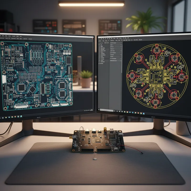
Every serious PCB design flow includes DFM (design-for-manufacturing) rule checks before releasing Gerber files to the fabricator. Tools like Siemens Valor, HyperLynx DFM, and various EDA-integrated DFM checkers validate the design against fabricator capabilities: minimum trace width, minimum spacing, minimum annular ring, drill aspect ratio, solder mask slivers, and dozens of other geometric rules.
These checks are essential, they catch design violations that would cause fabrication failure. But DFM rule checks and plating simulation answer fundamentally different questions, and confusing the two leaves a critical gap in the design-to-manufacturing workflow.
What DFM Rules Check
DFM rule checks are constraint-based: they compare design geometry against fabricator capability tables.
- Is the trace width above the fabricator’s minimum? (Pass/fail)
- Is the drill aspect ratio within the fabricator’s capability? (Pass/fail)
- Is the annular ring sufficient for drill registration tolerance? (Pass/fail)
- Are solder mask slivers above the fabricator’s minimum? (Pass/fail)
These checks are necessary conditions for manufacturability. A design that fails DFM rules cannot be fabricated. But passing DFM rules does not guarantee that the plating will be uniform.
What DFM Rules Cannot Predict
DFM rules operate on local design features, individual traces, individual vias, individual clearances. They do not model the panel-level electrochemical process that determines copper thickness.
No current distribution modelling. DFM rules do not compute the electric field distribution in the plating cell. They cannot predict that panel edges will plate 40% thicker than panel centres, or that a trace next to a large copper pour will plate 25% thinner than an isolated trace.
No via plating prediction. DFM rules check that the via aspect ratio is within the fabricator’s nominal capability. They do not predict the actual copper thickness at the via barrel midpoint, which depends on the specific plating cell geometry, chemistry, and current parameters, not just the aspect ratio.
No process parameter sensitivity. DFM rules are static constraints. They do not evaluate how changes in plating current density, pulse waveform, or flight bar position affect the copper distribution on a specific panel layout.
No copper balance assessment. DFM rules may flag a gross copper density imbalance (e.g., “Layer 3 copper density below 20%”), but they do not compute the electrochemical consequence of that imbalance or generate corrective thieving patterns.
What Plating Simulation Adds
Elsyca PCBPlate and PCBBalance provide the physics-based prediction that DFM rules cannot:
Quantitative thickness prediction. PCBPlate outputs copper thickness in micrometres at every point on the panel, traces, pads, vias, and thieving features. This is not a pass/fail check but a quantitative map that the designer and fabricator can use to evaluate process margin.
Via barrel analysis. PCBPlate predicts the thickness profile along the full via barrel length, identifying thin-barrel conditions that pass the DFM aspect ratio check but fail the reliability requirement.
Impedance impact. Combined with trace geometry and dielectric data, the PCBPlate thickness prediction can be used to compute the actual impedance at each controlled-impedance trace location, accounting for plating variation that DFM rules assume is zero.
Copper balance optimisation. PCBBalance generates simulation-optimised thieving patterns that the DFM rule check cannot produce. The thieving is designed for electrochemical uniformity, not just copper density balance.
The Recommended Workflow
DFM rule checks and plating simulation are complementary, not competing. The recommended sequence for Indian PCB design teams:
- DFM rule check (Valor, HyperLynx DFM): verify the design meets all fabricator geometric constraints. Fix any violations. This is the necessary precondition.
- PCBBalance: optimise copper balance across all layers for uniform plating.
Generate balanced Gerber files. 3. DFM rule check on balanced design: verify that the added thieving features do not violate any DFM rules (clearance, spacing). 4. PCBPlate: simulate the plating outcome for the balanced panel layout. Verify that copper thickness meets specification at all critical locations. 5. Release to fabrication with confidence that both design rules and plating physics are satisfied.
This five-step workflow takes more effort than a simple DFM check, but the payoff is boards that meet specification on the first fabrication run, reducing the iterative loop of fabricate-test-reject-redesign that consumes time and money.
Availability in India
GSAS provides both the DFM rule checking tools (Siemens Valor, HyperLynx DFM) and the plating simulation tools (Elsyca PCBPlate, PCBBalance) in India. This combination, available from a single engineering partner, gives Indian PCB design teams the complete design-to-manufacturing verification workflow.
Contact us from Bengaluru, Hyderabad, Chennai, Pune, Mumbai, Delhi NCR, or Visakhapatnam.
Explore Elsyca Products → | Explore Siemens EDA → | Request a Quote →
Also appears in:
Interested in Elsyca tools?
Talk to our application engineers for personalized tool recommendations.
More from Elsyca
View all →
Elsyca PCBPlate: How Panel Plating Simulation Predicts Copper Thickness Before Fabrication
5 Apr · 6 min

Elsyca PlatingManager: Digital Twin Simulation for Industrial Electroplating Lines
4 Apr · 5 min

Copper Thieving for PCBs: Why Manual Methods Fail and How Simulation Fixes It
3 Apr · 5 min

Via Plating Reliability: Why Thin Barrels Fail and How Simulation Prevents It
2 Apr · 5 min

Emulating Processor Power for Thermal Testing: Why Constant Power
7 Oct · 7 min

CRPS and Rack Power Supply Testing: The Six Tests That Matter
7 Oct · 7 min