
 Siemens EDA
 Xpedition Package Designer
IC PackagingIC package substrate and interposer layout for BGA, flip-chip, fan-out, and 2.5D/3D heterogeneous integration. Available in India from GSAS.
Package Types
BGA, QFN, flip-chip, wire-bond, fan-out WLP, 2.5D/3D
Routing
RDL routing, bump/ball assignment, via optimization
Die Placement
Multi-die placement for chiplet and heterogeneous designs
Co-Design
Package-to-board (Xpedition) and package-to-mechanical (NX)
Advanced Packaging
TSMC InFO, CoWoS, interposer, silicon bridge
Overview
About Xpedition Package Designer
Xpedition Package Designer from Siemens EDA is a dedicated IC package substrate and interposer layout tool that handles the full complexity of modern semiconductor packaging, from conventional wire-bond and BGA packages through advanced flip-chip, fan-out wafer-level, and 2.5D/3D heterogeneous integration technologies. As the semiconductor industry shifts toward chiplet architectures and advanced packaging to extend Moore’s Law, the package substrate has become as complex as a high-density PCB, requiring specialized design tools with IC-scale routing density and PCB-scale manufacturing awareness.
The tool provides die placement, bump and ball assignment, redistribution layer (RDL) routing, via structure definition, and design rule checking for multi-layer package substrates. It supports the full range of packaging technologies: traditional wire-bond and QFN packages, flip-chip BGA with high-density escape routing, fan-out wafer-level packaging (FOWLP), and advanced 2.5D interposer designs such as TSMC CoWoS and InFO. For chiplet-based designs, Xpedition Package Designer handles multi-die placement and routing on silicon interposers and organic substrates with heterogeneous die integration.
| Capability | Detail |
|---|---|
| Substrate Layout | Multi-layer substrate routing with IC-scale density |
| RDL Routing | Redistribution layer design for WLP and fan-out |
| Bump/Ball Assignment | Flip-chip bump and BGA ball map management |
| Die Placement | Multi-die and chiplet placement optimization |
| DRC | Package-specific design rule checking |
| Board Co-Design | Integrated with Xpedition PCB for package-board co-optimization |
| Mechanical Co-Design | NX integration for warpage and thermo-mechanical analysis |
| Advanced Packaging | CoWoS, InFO, silicon bridge, 3D stacking support |
The package-to-board co-design workflow with Xpedition PCB enables concurrent optimization of package pin-out and board routing, while the mechanical co-design workflow with NX provides warpage simulation and thermo-mechanical stress analysis for reliability prediction. This integrated approach is critical for advanced packages where package and board design decisions are tightly coupled.
GSAS Micro Systems provides Xpedition Package Designer licensing and technical support for semiconductor packaging teams across India, with guidance on advanced packaging flow setup, co-design methodology, and foundry packaging technology integration.
Buy Xpedition Package Designer in India: GSAS India-Wide Support
GSAS provides Xpedition Package Designer with INR invoicing, local FAE support, and Siemens maintenance and support across India:
- Bengaluru: Semiconductor design centres working on BGA and flip-chip substrate layout for mobile SoCs, AI accelerators, and HBM integration for data centre chips
- Hyderabad: Defence semiconductor packaging teams designing multi-chip modules for radar and EW processors, and fabless companies outsourcing advanced package substrate design
- Chennai: Automotive semiconductor packaging for ADAS SoCs and sensor fusion ICs requiring package-to-board co-design with thermal management
- Pune: Automotive IC packaging R&D for powertrain and BMS controllers, and industrial semiconductor companies designing SiP modules
- Mumbai: Semiconductor packaging teams supporting telecom infrastructure ICs and data centre accelerator programs with 2.5D interposer substrates
- Delhi NCR: Defence and space semiconductor groups designing radiation-hardened packages, and telecom IC packaging for 5G RF front-end modules
- Coimbatore: Industrial power management IC packaging teams designing QFN and BGA substrates for motor drive and power conversion applications
- Visakhapatnam: Naval defence electronics packaging teams designing multi-chip modules for sonar processors, and medical device IC packaging
- Vadodara: Power semiconductor packaging teams designing high-current substrates for industrial power modules
- Kolkata: Eastern India semiconductor design teams and academic packaging research groups
Contact sales@gsasindia.com or call +91 80 6590 1783 for evaluation licenses, co-design flow setup, and advanced packaging methodology workshops.
Blog
Siemens EDA Insights

India's EDA Moment: Why Design Tool Demand Is Growing, and the Engineering Careers It Creates
Electronic design automation is one of the few engineering markets where the global numbers and India's industrial policy are pointing the same direction at the same time. Here is what the published data actually says, which engineering roles the growth creates, and where GSAS Micro Systems fits as an authorized Siemens EDA engineering partner.

AI and Complexity Are Redrawing EDA: Siemens on the Trillion-Transistor Era
Siemens argues that chip complexity has outgrown siloed design and that the lines between chip, package and board can no longer be drawn. GSAS summarises the Industry Forward podcast episode and sets out what it changes for design teams in India: verify across the chip-to-board boundary before layout, not after the prototype.

Calibre Vision AI: Bringing Order to DRC Debug at Advanced Nodes
Siemens EDA's Calibre Vision AI turns full-chip DRC debug from an unmanaged flood of violations into a tracked, filtered, hand-off-able workflow. What Signal status tracking, global filters and shareable workspaces mean for Indian SoC teams.
Related products
More from Siemens EDA
All Siemens EDA products →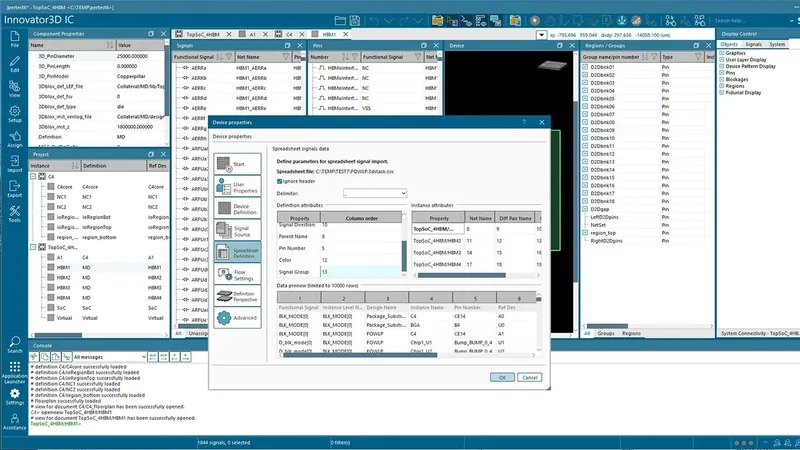
Innovator3D IC Layout
TSMC InFO-certified IC packaging layout tool for 2.5D/3D integration and advanced fan-out wafer-level packaging. Buy in India from GSAS with local support.
View Innovator3D IC Layout →
Calibre
Industry-standard IC physical verification and signoff platform, DRC, LVS, parasitic extraction, and pattern matching for advanced-node tapeout. Available in India from GSAS.
View Calibre →
Solido
Statistical variation-aware simulation and library characterization for advanced-node analog/mixed-signal IC design. Available in India from GSAS.
View Solido →Interested in Xpedition Package Designer?
Get pricing, an evaluation unit, or a technical consultation from our application engineers.