MIPI I3C Adoption in Indian Semiconductor Design Centers
MIPI Alliance lists I3C v1.0 as a 2016 release, with I3C v1.2 as the current version. MIPI describes I3C as “the successor to I2C, incorporating the key capabilities of legacy I2C and SPI interfaces into an advanced, consolidated specification”, offering “legacy compatibility with I2C (I3C and I2C devices can coexist on the same bus)” and a two-wire interface that “supports in-band interrupts which reduces pin count and signal paths”. MIPI also lists multi-controller support, dynamic addressing and command-code compatibility among the technical highlights.
A decade on from that first release, I3C adoption is accelerating, and India’s semiconductor design centers are at the center of that acceleration. Design teams in Bengaluru and Hyderabad are integrating I3C into SoCs, sensor hubs, camera interface modules, and power management ICs for mobile, automotive, and IoT applications.
Where I3C Fits in Indian Design Activity
India’s semiconductor design ecosystem is concentrated in a few high-activity areas where I3C adoption is most relevant:
Mobile SoC design. Several major mobile SoC vendors run significant design teams in Bengaluru and Hyderabad. Mobile SoCs were early adopters of I3C, using it for sensor hub communication (accelerometers, gyroscopes, magnetometers, proximity sensors) where I2C’s speed and interrupt limitations have been pain points. I3C’s in-band interrupt mechanism is particularly valuable in mobile, where reducing pin count directly impacts die size and package cost.
Automotive SoC and ADAS. India’s automotive semiconductor design activity is growing, with teams working on ADAS processors, body controllers, and battery management ICs. Automotive applications benefit from I3C’s higher bandwidth for sensor fusion (combining data from multiple sensors at higher update rates than I2C supports) and its multi-drop bus simplification compared to point-to-point sensor interfaces.
IoT and edge computing. Companies designing IoT SoCs and edge AI processors in India are evaluating I3C for sensor interfaces. Binho’s I3C Cafe describes I3C as offering “higher data rates (up to 12.5 Mbps in SDR mode), lower power consumption, and in-band interrupts while maintaining backward compatibility with I2C devices”, and that combination is what makes it attractive for battery-powered sensor platforms.
Sensor design. Indian design centers working on MEMS accelerometers, gyroscopes, pressure sensors, and environmental sensors are adding I3C interfaces to their next-generation parts. These sensors ship as I3C targets that need to be validated against the I3C specification before silicon tape-out and again during post-silicon bring-up.
Why Adoption Has Been Gradual
Despite its technical advantages, I3C adoption has been slower than the specification’s authors anticipated. The reasons are practical, not technical:
Tooling gap. Until recently, there was no practical bench tool for exercising I3C buses. Engineers designing I3C interfaces had to rely on FPGA-based prototypes or internal silicon to generate I3C traffic. This made I3C development significantly more difficult than I2C development, where inexpensive USB-to-I2C adapters have been available for decades.
Ecosystem inertia. I2C has a massive ecosystem of devices, tools, libraries, and engineering expertise. Every embedded engineer knows I2C. Switching to I3C requires new tools, new driver code, new validation procedures, and new engineering knowledge. The switching cost is real, even when the technical benefits are clear.
Mixed buses. Many real-world designs include both I3C and legacy I2C devices on the same bus (I3C supports this through backward-compatible mixed bus operation). Testing mixed buses adds complexity, the I3C controller must handle both protocol types, and validation must cover both I3C-native and I2C-legacy communication paths.
Specification complexity. I3C is a more complex protocol than I2C. Dynamic addressing, in-band interrupts, HDR modes, and the full CCC set create a larger state space for implementers to get right. Validation requires exercising more protocol corner cases than I2C.
The Tooling Turning Point
The Binho Supernova is one of the instruments that closes the tooling gap. Binho specifies:
- An I3C role of Controller or Target, across spec versions v1.0, v1.1.1 and v1.2, at up to 12.5 MHz
- SDR mode and HDR-DDR, with In-Band Interrupts, Hot-Join and all Common Command Codes
- An I3C signalling range of 0.8 V to 3.3 V, below the 1.2 V to 3.3 V of its I2C, SPI, UART and GPIO pins
- Cross-platform software: the Mission Control GUI plus Python, C, C++ and C# SDKs
Passive decoding is a separate Binho product: the I3C Basic Protocol Analyzer plugin for Saleae Logic, which is licensed software rather than a free download.
For pre-silicon validation teams in Bengaluru and Hyderabad, the Supernova provides an external I3C controller for exercising I3C target IP in FPGA prototypes. For post-silicon teams, it provides the bus access needed to bring up I3C interfaces on first silicon. For sensor companies, it provides the test infrastructure for validating I3C target devices against the specification.
What Indian Design Teams Need
Based on conversations with engineering teams across India’s semiconductor design centers, the I3C development needs are consistent:
Interactive bus access. Engineers want to talk to I3C devices interactively, scan the bus, assign addresses, read registers, exercise CCCs, without writing driver code. Mission Control provides this through a GUI interface.
Scriptable test sequences. Validation requires repeatable test sequences that exercise specific protocol scenarios: ENTDAA with multiple targets, IBI handling under bus load, HDR-DDR transfers with varying payload sizes. The Python SDK enables these scripts.
Protocol visibility. When something goes wrong on the I3C bus, engineers need to see the raw protocol transactions, what was sent, what was received, where the protocol diverged from expectations. The Supernova’s Saleae integration provides this visibility.
Mixed-bus testing. Designs that include both I3C and I2C devices need a single tool that handles both protocols. The Supernova’s I2C and I3C support from one device addresses this directly.
Why Buy from GSAS
GSAS Micro Systems is an authorized Binho engineering partner in India. We provide the Supernova to semiconductor design teams across Bengaluru, Hyderabad, Chennai, Pune, Mumbai, and Delhi NCR with INR invoicing, local inventory, and I3C-specific applications engineering support. Whether your team is validating I3C IP in an FPGA, bringing up first silicon, or testing I3C sensor devices, our engineers can assist with bus architecture, tool setup, and validation methodology. Contact us for evaluation units or a technical consultation.
Also appears in:
Interested in Binho tools?
Talk to our application engineers for personalized tool recommendations.
More from Binho
View all →
I3C FAQ for Firmware Teams: What the Bus Is, What Changes, and What You Need on the Bench
31 Jul · 8 min
Running the Binho Supernova as an I3C Target: Emulating a Device Against Your Own Controller
31 Jul · 7 min
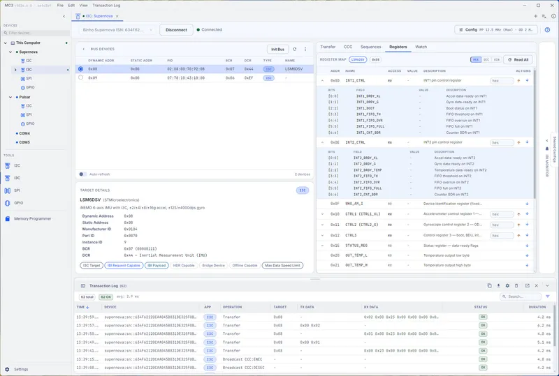
Binho Mission Control 3 (Public Preview): Point-and-Click I2C, SPI, I3C, and GPIO
20 Jul · 5 min
Binho Mission Control: Point-and-Click I2C, SPI, and UART Without Writing Code
7 Apr · 5 min

Emulating Processor Power for Thermal Testing: Why Constant Power
7 Oct · 7 min

CRPS and Rack Power Supply Testing: The Six Tests That Matter
7 Oct · 7 min