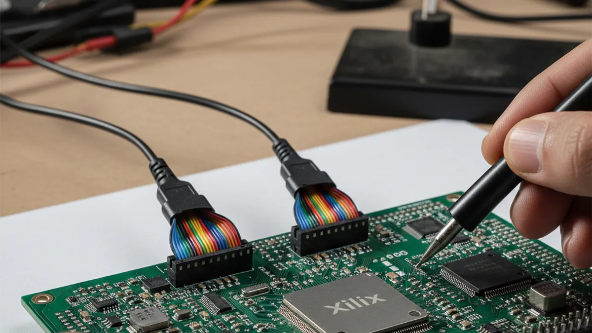
The JTAG programming cable is one of the smallest line items on an FPGA bench or a production fixture, and one of the easiest to get wrong. The wrong cable costs a day of debugging that has nothing to do with your design, or worse, becomes the silent bottleneck that caps the throughput of an entire production line. Digilent makes two high-speed USB JTAG cables that cover the range from R&D bench to production fixture: the JTAG-HS2 and the JTAG-HS3. Many development boards also ship with an on-board USB programmer.
This guide is written for the three groups of engineers who reach for these cables most often in India: memory device validation and characterization teams building DDR5/HBM test benches around AMD/Xilinx FPGAs; defence and aerospace electronics manufacturers programming FPGAs into avionics, radar, and EW systems on Indian production lines; and high-volume electronics manufacturing (EMS) lines that configure and flash-program FPGAs at volume and run JTAG boundary-scan structural test on every assembled board. It covers what each cable does, where IEEE 1149.1 boundary scan fits, how to think about production FPGA programming, and which cable maps to which job.
What a JTAG Programming Cable Actually Does
A JTAG cable connects a host PC to the target’s JTAG chain (TCK, TMS, TDI, TDO) and lets the AMD/Xilinx toolchain, iMPACT, ChipScope, EDK, or Vivado, configure the FPGA, program configuration memory, and run hardware debug. The same four-wire interface is the access port for IEEE 1149.1 boundary-scan structural test on the assembled PCB. Two specs dominate the cable decision:
- Target voltage range: the cable must level-shift to your FPGA’s I/O bank voltage (1.8 V, 2.5 V, 3.3 V, or 5 V logic).
- Speed: how fast it shifts the JTAG bitstream, which sets your programming, reconfiguration, and boundary-scan vector time.
Both Digilent cables cover 1.8 V to 5 V and run at up to 30 Mbit/s, so they share the same voltage and speed envelope. The differences are in connectors, buffering, and one debug feature that matters specifically for Zynq. Everything below builds on those shared specs, they are the same on the bench, on the validation rig, and on the production line.
Digilent JTAG-HS2: The Flexible Bench and Production Cable
The JTAG-HS2 is the more versatile of the two. It is a high-speed programming solution for AMD FPGAs, fully compatible with all AMD tools (iMPACT, ChipScope, EDK) and supported by Digilent’s Adept software and Adept SDK.
What sets the HS2 apart:
- Target voltage 1.8 V to 5 V, level-shifted via a separate Vdd pin
- Up to 30 Mbit/s (modes 0 and 2; 2 Mbit/s in modes 1 and 3)
- 24 mA three-state buffers that drive long or heavily loaded JTAG chains where slimmer cables struggle
- Two connector options included: Digilent’s 6-pin 100-mil header and AMD’s 2x7 2 mm connector (adapter in the box)
- IEEE 1149.7-2009 Class T0–T4, including 2-wire JTAG
- Host link over USB 2.0 Micro-AB
Choose the HS2 when you want connector flexibility (it drops onto both the Digilent header footprint and AMD’s 2x7), strong drive for long or multi-device chains, or 2-wire JTAG support. The Adept SDK gives it a command-line, scriptable programming path, which is what makes it equally at home as a general-purpose bench cable for Artix-7, Spartan, and Kintex targets and as the programming head in a production test fixture.
Digilent JTAG-HS3: The Faster, Slimmer Zynq Specialist
The JTAG-HS3 is an affordable, slim high-speed cable that adds one capability the HS2 lacks: it builds on the earlier JTAG-HS1 by adding an open-drain buffer on pin 14, which lets debugging software reset the processor core (PS) of AMD’s Zynq SoC platform during a debug session.
Its profile:
- Vref 1.8 V to 5 V, up to 30 Mbit/s (user-adjustable frequency)
- Open-drain pin-14 buffer for Zynq PS_SRST_B core reset
- AMD 2x7 2 mm connector (no 6-pin header)
- Host link over High-Speed USB 2.0 Micro-B
- Compatible with AMD ISE 14.1+ and Vivado 2013.3+, plus iMPACT, ChipScope, EDK
Choose the HS3 when your work centers on Zynq-7000 SoC bring-up and you need clean, repeatable processor-system resets between Vivado debug runs, at a lower cost and slimmer footprint than the HS2. The user-adjustable clock means you can push the frequency up on a clean, short chain to shorten the configuration window, or dial it back for a long or noisy one.
JTAG Boundary-Scan and IEEE 1149.1 Structural Test on the Production Line
For EMS and defence manufacturing teams, the JTAG chain is not only a programming path, it is the IEEE 1149.1 boundary-scan access port for structural test of the assembled PCB. Boundary scan shifts test vectors into and out of the boundary-scan register of every compliant device on the chain, letting you check solder joints, opens, shorts, and net-level connectivity on dense or BGA-heavy assemblies that a flying-probe or bed-of-nails fixture cannot reach. On an FPGA-centric board, the FPGA itself is the anchor of the boundary-scan chain, and the cable is what drives it.
What the JTAG cable contributes to a boundary-scan / structural-test setup:
- Reliable drive on long, multi-device chains. Production boards rarely have a single FPGA, they chain the FPGA with CPLDs, configuration PROMs, and other 1149.1-compliant devices. The HS2’s 24 mA three-state buffers are sized for exactly this: long or heavily loaded chains where a slimmer cable’s drive runs out. This is the cable’s single most relevant property for boundary-scan structural test.
- Correct level-shifting across mixed-voltage boards. A board with 1.8 V FPGA I/O banks, 2.5 V interface logic, and 3.3 V legacy parts needs the cable to track the JTAG chain’s logic level. Both cables level-shift across the 1.8 V to 5 V range, so the same cable works whether you are testing a low-voltage controller board or a mixed-voltage system board.
- The same chain that tests the board also configures it. Structural test and FPGA configuration ride the same TCK/TMS/TDI/TDO pins, so one cable on one fixture connection covers both the IEEE 1149.1 boundary-scan pass and the FPGA configuration / flash-programming step.
For PCB-assembly structural test, the boundary-scan vectors themselves come from your test tool of choice, the cable is the physical access layer that drives them onto the chain. The HS2’s connector flexibility (both the Digilent 6-pin header and the AMD 2x7) and its 24 mA drive make it the natural pick for a manufacturing-test fixture that has to reach a variety of board designs.
Production and High-Volume FPGA Configuration and Flash Programming
When you move from one board on a bench to hundreds or thousands of boards on a line, the question changes from “does it work” to “does it work the same way every single time, without a human in the loop.” This is the world of production FPGA programming and high-volume FPGA configuration, and it is where the cable’s scriptability and speed start to matter as much as its electrical specs.
Repeatable, scriptable programming. The HS2 is supported by Digilent’s Adept SDK, which exposes a command-line and scripted programming path. That is the hook a production-test executive needs: the line controller (a Python or C# test stack, or a home-grown fixture controller) calls the same programming command for every board, programs the FPGA configuration memory, verifies, and moves on. No operator clicking through a GUI, no per-board variation. Repeatability is the whole point, a scripted Adept flow programs board number 5,000 byte-identically to board number 1.
When to step up from the bench cable (HS2) to the faster path. Both cables top out at the same 30 Mbit/s, so neither is “the fast one” on raw spec. Where the HS3 helps is its user-adjustable frequency: on a clean, short production chain you can run it up to shorten the per-board configuration window, which is exactly the lever you want when programming time sits on the critical path of a high-volume line. The HS2, by contrast, earns its place on lines with long or multi-device chains, mixed connector footprints, or 2-wire JTAG targets, where its 24 mA buffers and dual connectors matter more than shaving the clock. The honest rule of thumb: pick the HS2 when the fixture’s electrical demands (chain length, drive, connector variety) dominate, and consider the HS3 when the chain is short and clean and you want to push the clock to compress configuration time.
FPGA flash programming for field-deployed units. Production programming is not only about the line. Custom hardware that ships without an embedded programmer still needs configuration memory written, and re-written when firmware updates land in the field. Either cable handles FPGA flash programming of the on-board configuration memory; the HS2’s scriptable Adept path makes it the easier one to wrap into a documented, repeatable re-flash procedure for service teams.
FPGA-Based Memory (DDR5/HBM) Validation and Characterization Benches
Memory device validation and characterization teams build test benches around an FPGA that acts as the controller and traffic generator for the device under test, driving DDR5 or HBM transactions, sweeping timing and voltage corners, and logging margins. The validation rig lives or dies on repeatability: every run has to start from the same known FPGA state so that the only thing changing between sweeps is the memory parameter under test.
Where the cable fits in a memory-validation test bench:
- Configuring and flashing the controller FPGA. The first step in any bench session is getting the right bitstream onto the AMD/Xilinx controller FPGA on the test board. A dedicated cable gives the bench engineer a clean, external programming path independent of whatever the board’s on-board programmer does, important when the test board is a custom characterization fixture rather than an off-the-shelf dev board. Both cables configure the FPGA and program its configuration memory over the standard JTAG chain at up to 30 Mbit/s.
- Mixed-voltage rigs. Characterization fixtures routinely mix the FPGA’s I/O bank voltage with separate interface and memory-side rails. The 1.8 V to 5 V level-shifting range, fed from a separate Vdd reference, lets one cable track the JTAG chain’s logic level across the rig without re-jumpering.
- Drive for instrumented boards. A characterization board is rarely minimal, it carries the FPGA plus probe points, level translators, and often additional scan-chain devices. The HS2’s 24 mA three-state buffers give the headroom to drive that loaded chain reliably, which is why it tends to be the default on a memory-validation bench.
- Scriptable bring-up between runs. When the validation campaign needs to reconfigure the FPGA between corner sweeps, a different controller build, a different traffic pattern, the HS2’s Adept SDK scripting lets the test automation reflash the FPGA as a step in the sequence rather than a manual interruption.
For a memory-validation bench, the HS2 is usually the right default: its connector flexibility and high drive suit instrumented custom test boards, and its scriptable programming path slots into the automation that already drives the rig. If the controller FPGA is a Zynq-7000 SoC and the campaign involves software running on the PS, the JTAG-HS3’s pin-14 PS reset earns its place for clean processor-system resets between runs.
Defence and Aerospace FPGA Programming on Indian Production Lines
Defence and aerospace electronics manufacturers program AMD/Xilinx FPGAs into avionics, radar, electronic-warfare, and other rugged systems on Indian production lines. The governing requirements here are repeatability, controlled configuration, and a documented, auditable programming step: the same bitstream, programmed the same way, verified the same way, on every unit, with a record that survives a quality audit.
How the cable supports controlled, repeatable defence and aerospace FPGA configuration:
- Repeatable, scripted configuration. A defence production line cannot depend on an operator’s judgement at the programming station. The HS2’s Adept SDK command-line path lets the line wrap FPGA configuration and flash programming into a fixed, version-controlled script, the configuration step becomes a deterministic part of the build travel, not a manual operation.
- Boundary-scan structural test on rugged assemblies. Avionics and radar boards are dense, conformally coated, and frequently BGA-heavy, which is exactly the assembly class where physical-probe access falls short and IEEE 1149.1 boundary scan becomes the structural-test method of record. The same JTAG cable that configures the FPGA drives the boundary-scan chain for that structural test.
- Drive and connector flexibility for mixed system boards. Rugged system boards chain the FPGA with multiple compliant devices across mixed voltage rails. The HS2’s 24 mA three-state buffers and 1.8 V to 5 V range cover long, mixed-voltage chains; its two included connectors (Digilent 6-pin header and AMD 2x7) let one cable type serve a variety of board designs across a programme.
- Zynq-based subsystems. Where the rugged design is built on a Zynq-7000 SoC, common in radar and signal-processing subsystems, the JTAG-HS3’s open-drain pin-14 buffer provides the clean PS core reset needed for repeatable processor-system bring-up.
This maps directly to the kind of work GSAS supports for aerospace and defence electronics teams in India: controlled, documented FPGA configuration and JTAG structural test, with cables and application support sourced locally with INR invoicing.
When the On-Board Programmer Is Enough (and When It Isn’t)
Most Digilent development boards, the Arty A7, Basys 3, Zybo Z7, and others, include an on-board USB-JTAG programmer. For early development on a dev board, that is all you need; there is no reason to add an external cable.
You move to a dedicated JTAG-HS2 or HS3 when:
- You build custom hardware: a characterization test board, a rugged system card, a production assembly, that ships without an embedded programmer
- You need production programming in a test fixture (the Adept SDK scripts the HS2 for repeatable, automated line programming)
- You run IEEE 1149.1 boundary-scan structural test and need a cable with the drive to sit on a long, multi-device chain
- You require in-field re-flashing of deployed units
- The on-board programmer is too slow, lacks drive for a long chain, or cannot reset a Zynq PS core (HS3)
HS2 vs HS3: Which Should You Choose?
Both cables share the 1.8 V to 5 V range and 30 Mbit/s ceiling, so the choice is rarely about raw voltage or top speed. It is about connectors, drive, the Zynq PS reset, and which job is on your bench or line. Map your use case to the cable:
| Your use case | Recommended cable | Why |
|---|---|---|
| Memory (DDR5/HBM) validation / characterization bench | JTAG-HS2 | High 24 mA drive for instrumented test boards, connector flexibility, scriptable Adept reflash between corner sweeps |
| Memory validation bench with a Zynq-7000 controller | JTAG-HS3 | Pin-14 PS core reset for clean processor-system resets between runs |
| EMS / high-volume production FPGA flash programming | JTAG-HS2 | Adept SDK scripting for repeatable, automated line programming; dual connectors fit varied board designs |
| Short, clean production chain where config time is the bottleneck | JTAG-HS3 | User-adjustable frequency to push the clock and compress the per-board configuration window |
| IEEE 1149.1 boundary-scan structural test on dense assemblies | JTAG-HS2 | 24 mA three-state buffers drive long, multi-device chains reliably |
| Defence / aerospace FPGA configuration on a production line | JTAG-HS2 | Repeatable scripted configuration, high drive, connector flexibility for mixed system boards |
| Zynq-7000 subsystem bring-up (radar, signal processing, SoC) | JTAG-HS3 | Open-drain pin-14 buffer resets the Zynq PS core during Vivado debug |
| Custom Artix-7 / Spartan / Kintex board bring-up | JTAG-HS2 | General-purpose drive, both connectors, 2-wire JTAG support |
| Early development on a Digilent dev board | On-board programmer | Already integrated, no external cable needed |
Side-by-Side Comparison
| Feature | JTAG-HS2 | JTAG-HS3 | Typical on-board programmer |
|---|---|---|---|
| Target voltage | 1.8 V – 5 V | 1.8 V – 5 V | Fixed to board |
| Max speed | 30 Mbit/s | 30 Mbit/s | Varies |
| Connectors | 6-pin header + AMD 2x7 | AMD 2x7 | Soldered to board |
| Buffers | 24 mA three-state | Standard | n/a |
| 2-wire JTAG | Yes (IEEE 1149.7) | No | No |
| Zynq PS reset (pin 14) | No | Yes | Board-dependent |
| Host USB | USB 2.0 Micro-AB | USB 2.0 Micro-B | On board |
| Scripted programming | Adept SDK (command-line) | AMD toolchain | Board-dependent |
| Best for | Custom boards, long chains, boundary scan, production | Zynq SoC debug, short clean chains, budget | Dev-board prototyping |
Frequently Asked Questions
Do the JTAG-HS2 and HS3 work with Vivado? The JTAG-HS3 is explicitly compatible with AMD Vivado 2013.3 and newer (and ISE 14.1+). Both cables work with the classic AMD tools, iMPACT, ChipScope, and EDK, and the HS2 is supported by Digilent’s Adept software and Adept SDK for scripted, command-line programming.
Can these cables run IEEE 1149.1 boundary-scan structural test? The cable is the physical access layer onto the JTAG chain (TCK, TMS, TDI, TDO) that IEEE 1149.1 boundary scan uses. The boundary-scan vectors themselves come from your test tool; the cable drives them onto the chain. The HS2’s 24 mA three-state buffers are sized for the long, multi-device chains common on production assemblies, which is why it is the usual choice for a manufacturing-test fixture.
Which cable is better for high-volume production FPGA programming? For repeatable, scriptable line programming the HS2 is the usual choice, because the Adept SDK gives it a command-line path a production-test executive can call for every board. If the production chain is short and clean and configuration time is on the critical path, the HS3’s user-adjustable frequency lets you push the clock to compress the per-board window. Both cables top out at 30 Mbit/s.
Which cable should I use for a memory validation or characterization bench? The HS2, in most cases, its high 24 mA drive suits instrumented custom test boards, and its scriptable Adept path lets test automation reflash the controller FPGA between corner sweeps. If the controller FPGA is a Zynq-7000 SoC, the HS3 adds the pin-14 PS reset for clean processor-system resets between runs.
Which cable should I use for a Zynq-7000 board? The JTAG-HS3. Its open-drain pin-14 buffer resets the Zynq processor-system core during debug, which the HS2 does not provide. For non-Zynq Artix-7/Kintex targets, the HS2’s connector flexibility and higher drive make it the better all-round choice.
Can these cables program FPGAs from other vendors? The JTAG-HS2 and HS3 are designed and validated for AMD (formerly Xilinx) FPGAs and SoCs using AMD tools. For non-AMD targets, use the vendor’s recommended programmer.
What does a Digilent JTAG cable cost in India? Final INR pricing depends on quantity, GST, and exchange rates. GSAS Micro Systems issues formal quotations with GeM, SAP Ariba, Coupa, and TReDS support. Request a quote for current JTAG-HS2 and JTAG-HS3 pricing.
How do I buy the JTAG-HS2 or HS3 in India? GSAS Micro Systems is an authorized Digilent engineering partner in India. Buy either cable with INR invoicing, local stock guidance, and FPGA/Zynq bring-up support. Use Request Quote to get pricing and lead time.
Buy Digilent JTAG Cables in India from GSAS
For FPGA bring-up, memory-validation benches, boundary-scan structural test, and production FPGA programming, the right cable saves real time on the bench and protects throughput on the line. GSAS Micro Systems supplies the Digilent JTAG-HS2 and JTAG-HS3 with INR invoicing and AMD/Xilinx application support for memory-validation, defence and aerospace, and high-volume manufacturing teams across Bengaluru, Chennai, Hyderabad, Pune, Mumbai, and Delhi NCR. Request a quote for the JTAG programmer that fits your FPGA configuration, boundary-scan, and production-test workflow.
Also appears in:
Interested in Digilent tools?
Talk to our application engineers for personalized tool recommendations.
More from Digilent
View all →
Real-World SDR Applications: 5G Research, Satellites, IoT and ADS-B
28 Aug · 6 min
What Is Software Defined Radio (SDR)? A Practical Explainer for Indian Engineering Teams
19 Aug · 9 min

ZedBoard FPGA-in-the-Loop: HDL Verifier vs HDL Coder
5 Aug · 9 min

AI Data Centers in India: Test, Measurement & Memory Boom
4 Jun · 14 min

Emulating Processor Power for Thermal Testing: Why Constant Power
7 Oct · 7 min

CRPS and Rack Power Supply Testing: The Six Tests That Matter
7 Oct · 7 min