
 Elsyca
 Elsyca PCBBalance
PCB Design & ManufacturingAutomated PCB copper balancing DFM software, generates optimized Gerber files with uniform plating thickness. India licensing and support from GSAS.
Function
Automated copper thieving and balancing
Input
Extended Gerber (RS-274X) files
Output
Balanced Gerber files, HTML reports
Visualization
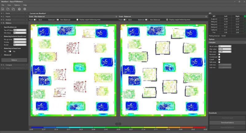
Color-coded thickness distribution plots
HDI Support
v2.1 with HDI layer stack handling
Overview
About Elsyca PCBBalance
Elsyca PCBBalance is an automated design-for-manufacturing (DFM) tool that optimizes copper distribution across PCB layers to achieve uniform electroplating thickness. The software reads Extended Gerber input files, analyzes copper density patterns across each layer, and automatically generates copper thieving and balancing features that equalize the current distribution during the plating process. The result is a set of production-ready Gerber files with optimized copper balance, reducing plating thickness variation and improving manufacturing yield.
| Feature | Specification |
|---|---|
| Function | Automated copper thieving and balancing |
| Input Format | Extended Gerber (RS-274X) |
| Output Format | Balanced Gerber files ready for production |
| Analysis | Copper density distribution per layer |
| Visualization | Color-coded plating thickness distribution plots |
| Reporting | HTML reports with KPI metrics per layer |
| HDI Support | v2.1 handles HDI layer stacks and microvias |
| Thieving Patterns | Dots, lines, grids, configurable size and spacing |
| Clearance Rules | User-defined keep-out zones and clearance to active copper |
| Batch Processing | Multi-layer, multi-panel automated workflow |
Non-uniform copper distribution is one of the most common causes of plating thickness variation in PCB manufacturing. Areas with low copper density receive disproportionately high current during electroplating, leading to excessive copper buildup, while dense copper regions may be under-plated. This variation affects impedance control, via reliability, and surface planarity, all critical for high-frequency and HDI designs. Traditional manual copper balancing is time-consuming, inconsistent, and often insufficient for today’s complex multi-layer boards.
PCBBalance eliminates manual copper balancing by automating the entire process. The software calculates the optimal placement of thieving features, dots, lines, or grid patterns, on each layer to equalize copper density and current distribution. Color-coded thickness distribution plots provide immediate visual feedback on the expected plating uniformity, while HTML reports quantify improvement through KPIs such as thickness range, standard deviation, and Cpk metrics. Engineers can evaluate the impact of balancing before sending files to the fabricator, catching DFM issues at the design stage rather than during production.
The v2.1 release extends PCBBalance capabilities to HDI layer stacks with sequential lamination, addressing the unique copper balancing challenges of microvia layers, buried vias, and asymmetric copper distributions that arise in advanced HDI designs. Support for Extended Gerber input ensures compatibility with all major EDA tools including Cadence Allegro, Altium Designer, Mentor PADS, and Zuken CR-8000.
PCB fabricators, EMS companies, and design teams responsible for DFM sign-off use PCBBalance to reduce plating rejection rates, improve impedance consistency, and shorten the design-to-manufacturing handoff cycle. The automated workflow processes entire panel layouts in minutes, replacing hours of manual copper fill work that varies between individual CAM engineers.
GSAS Micro Systems is an authorized Elsyca partner in India, providing PCBBalance licensing, DFM workflow integration support, and training for PCB design and manufacturing engineering teams across electronics companies and PCB fabrication shops.
Blog
Elsyca Insights
Elsyca PCBPlate: How Panel Plating Simulation Predicts Copper Thickness Before Fabrication
Elsyca PCBPlate simulates the electrochemical plating process to predict copper thickness distribution across PCB panels with 90%+ validated accuracy. Here is how it works and why Indian PCB manufacturers and designers need it.
Elsyca PlatingManager: Digital Twin Simulation for Industrial Electroplating Lines
Industrial electroplating, decorative chrome, hard chrome, zinc-nickel, copper, nickel, and tin plating of 3D parts, has traditionally been an empiric...
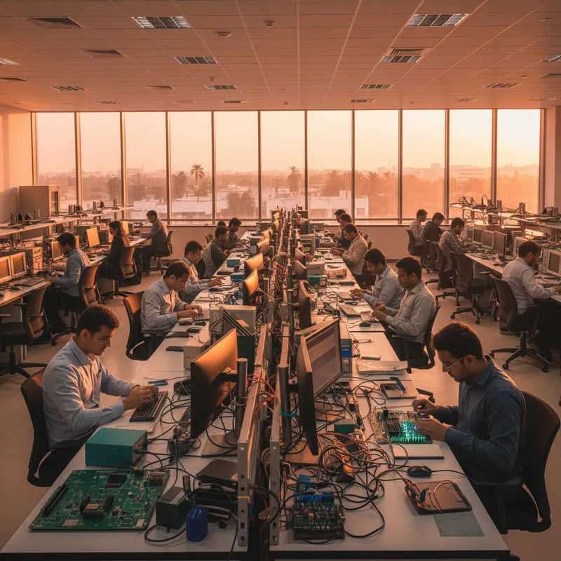
Copper Thieving for PCBs: Why Manual Methods Fail and How Simulation Fixes It
Copper thieving is the standard DFM technique for improving plating uniformity, but manual thieving patterns are crude approximations. Elsyca PCBBalance automates copper balancing using electrochemical simulation, delivering uniform plating that manual methods cannot achieve.
Related products
More from Elsyca
All Elsyca products →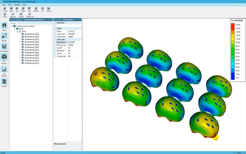
PlatingManager
Electroplating process simulation for predicting coating thickness distribution and optimizing rack layout, anode geometry, and current waveforms. Authorized India partner, GSAS Micro Systems.
View PlatingManager →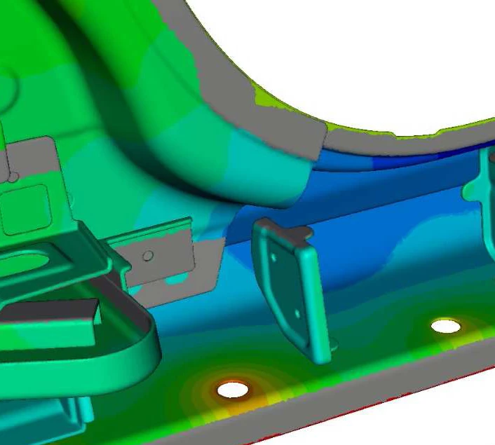
ECoatMaster
E-coating simulation for automotive body-in-white structures, predicting film thickness in complex cavities to eliminate bare spots. India pricing and local support from GSAS.
View ECoatMaster →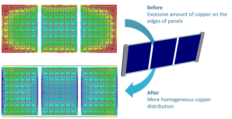
Elsyca PCBPlate
PCB panel and pattern plating simulation platform with 90%+ validated accuracy for copper thickness distribution. Buy in India from GSAS.
View Elsyca PCBPlate →Interested in Elsyca PCBBalance?
Get pricing, an evaluation unit, or a technical consultation from our application engineers.