
 Elsyca
 Elsyca PCBPlate
PCB Design & ManufacturingPCB panel and pattern plating simulation platform with 90%+ validated accuracy for copper thickness distribution. Buy in India from GSAS.
Function
Panel and pattern plating simulation
Accuracy
90%+ validated (Eurocircuits)
Input
Extended Gerber (RS-274X) files
Simulation
Flight bar position and anode modeling
Reports
ISO-compliant thickness distribution reports
Overview
About Elsyca PCBPlate
Elsyca PCBPlate is a simulation platform for predicting copper thickness distribution during PCB panel plating and pattern plating processes. The software models the electrochemical deposition environment, including flight bar position, anode geometry, bath chemistry, and current distribution, to generate accurate thickness predictions across the entire panel before a single board enters the plating line. Validated by Eurocircuits with over 90% accuracy compared to cross-section measurements, PCBPlate provides the quantitative foundation for plating process optimization.
| Feature | Specification |
|---|---|
| Simulation Types | Panel plating, pattern plating |
| Input Format | Extended Gerber (RS-274X) |
| Accuracy | 90%+ validated against cross-section measurements (Eurocircuits) |
| Flight Bar Modeling | Position, contact point, and current feed optimization |
| Anode Geometry | Anode shape, placement, and shielding configuration |
| Panel History | Full plating sequence simulation across process steps |
| Current Distribution | Primary, secondary, and tertiary current modeling |
| Thickness Output | 3D copper thickness maps across panel and individual boards |
| Reporting | ISO-compliant thickness distribution reports with statistical analysis |
| Batch Mode | Multi-panel, multi-recipe automated simulation |
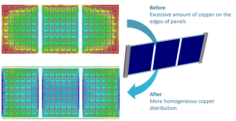
Copper thickness uniformity across a PCB panel directly impacts electrical performance, via reliability, and impedance control. During panel plating, boards near the panel edges and corners receive different current densities than those in the center, resulting in systematic thickness variation. Pattern plating introduces additional complexity because the copper density of the etched pattern affects local current distribution. These variations are difficult to predict empirically and often require multiple production trials to optimize, wasting material, time, and production capacity.
PCBPlate replaces trial-and-error plating optimization with physics-based simulation. Engineers define the panel layout, Gerber data, flight bar position, anode arrangement, and bath parameters; PCBPlate calculates the current distribution and resulting copper deposition across the entire panel surface. The software models both panel plating (uniform copper deposition on un-patterned panels) and pattern plating (selective deposition on etched circuit patterns), accounting for the complex interactions between copper density, resist openings, and current distribution that determine final thickness.
The full panel history feature tracks copper thickness through multiple sequential plating steps, from initial electroless deposition through panel plating and pattern plating, giving process engineers visibility into how each step contributes to the final thickness distribution. Flight bar position modeling reveals how mechanical contact points and current feed locations affect plating uniformity, enabling optimization of bar design and panel orientation.
PCB fabricators use PCBPlate to optimize their plating lines for new board designs, reducing the number of production trials needed to meet thickness specifications. Process engineers evaluate the impact of changing anode geometry, bath chemistry, or current density profiles before implementing changes on the production floor. Quality engineers use ISO-compliant reporting to document process capability and compliance with customer thickness requirements.
GSAS Micro Systems is an authorized Elsyca partner in India, providing PCBPlate licensing, plating process simulation consulting, and training for PCB fabrication process engineering teams.
Blog
Elsyca Insights
Elsyca PCBPlate: How Panel Plating Simulation Predicts Copper Thickness Before Fabrication
Elsyca PCBPlate simulates the electrochemical plating process to predict copper thickness distribution across PCB panels with 90%+ validated accuracy. Here is how it works and why Indian PCB manufacturers and designers need it.
Elsyca PlatingManager: Digital Twin Simulation for Industrial Electroplating Lines
Industrial electroplating, decorative chrome, hard chrome, zinc-nickel, copper, nickel, and tin plating of 3D parts, has traditionally been an empiric...

Copper Thieving for PCBs: Why Manual Methods Fail and How Simulation Fixes It
Copper thieving is the standard DFM technique for improving plating uniformity, but manual thieving patterns are crude approximations. Elsyca PCBBalance automates copper balancing using electrochemical simulation, delivering uniform plating that manual methods cannot achieve.
Related products
More from Elsyca
All Elsyca products →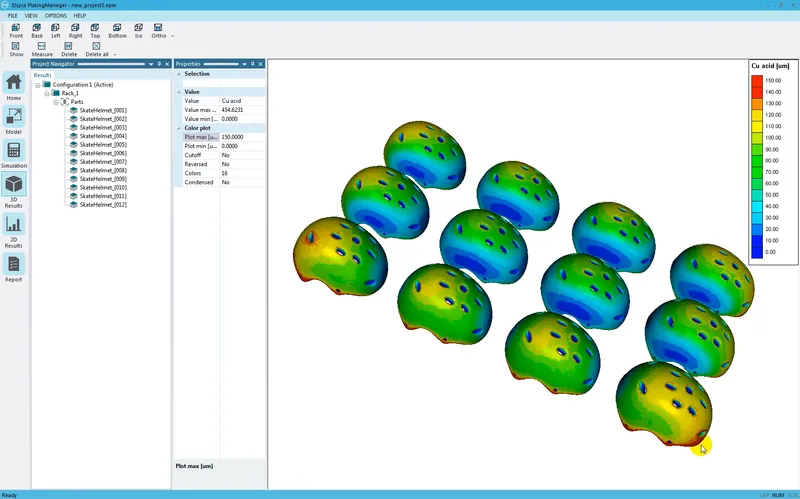
PlatingManager
Electroplating process simulation for predicting coating thickness distribution and optimizing rack layout, anode geometry, and current waveforms. Authorized India partner, GSAS Micro Systems.
View PlatingManager →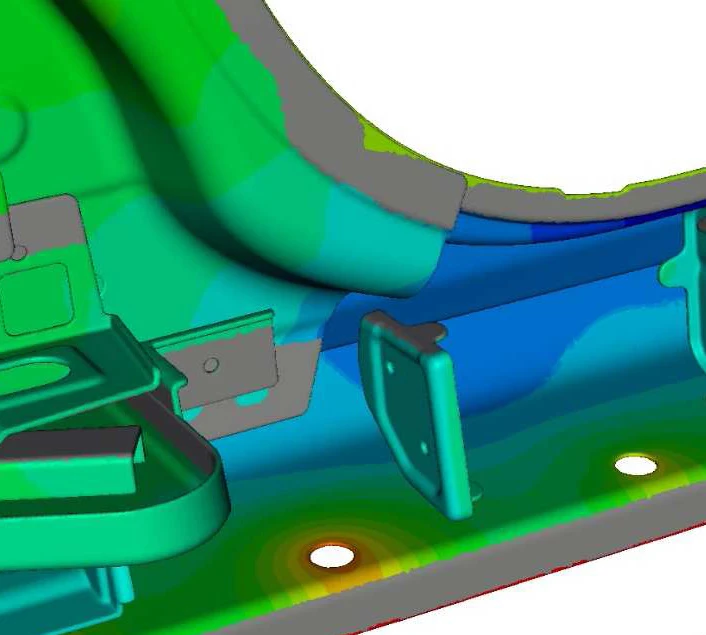
ECoatMaster
E-coating simulation for automotive body-in-white structures, predicting film thickness in complex cavities to eliminate bare spots. India pricing and local support from GSAS.
View ECoatMaster →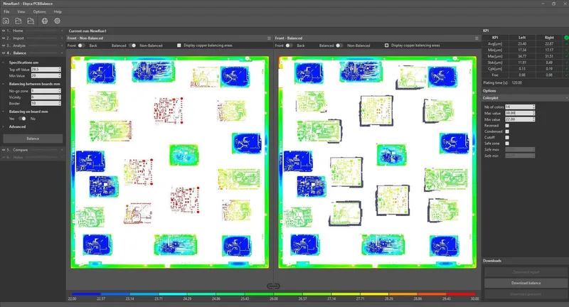
Elsyca PCBBalance
Automated PCB copper balancing DFM software, generates optimized Gerber files with uniform plating thickness. India licensing and support from GSAS.
View Elsyca PCBBalance →Interested in Elsyca PCBPlate?
Get pricing, an evaluation unit, or a technical consultation from our application engineers.