GSAS Micro Systems has announced a partnership with Elsyca NV to bring advanced PCB plating and design-for-manufacturing simulation tools to India’s electronics and manufacturing sector.
About Elsyca
Elsyca provides simulation-driven tools for electrochemical processes, specifically copper plating optimization for PCB manufacturing. Their solutions help PCB designers and manufacturers predict plating outcomes before production, reducing waste and iterations.
Solutions Now Available Through GSAS
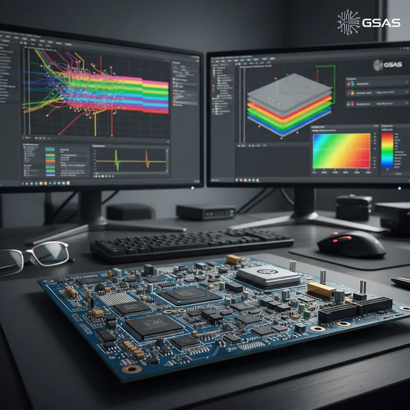
- PCBPlate: simulate copper thickness distribution across patterns, panels, and vias at the design stage
- PCBBalance: automated copper balancing for production-ready designs with fewer iterations
- PlatingManager: digital twin simulation of plating lines to predict and optimize manufacturing results
- IntelliTool: intelligent tooling optimization for plating process parameters
Why This Partnership Matters
Indian PCB manufacturers and design houses can now get early visibility into plating quality issues, before committing to expensive production runs. The result: reduced material waste, improved yield, and faster delivery cycles.
This partnership complements GSAS’s existing Siemens EDA portfolio (Xpedition, HyperLynx, Valor) by adding the electrochemical manufacturing simulation dimension that bridges the gap between PCB design and PCB fabrication.
Learn more about Elsyca | Request a demo
See the Original Post on LinkedIn
Also appears in:
Interested in Elsyca tools?
Talk to our application engineers for personalized tool recommendations.
More from Elsyca
View all →
Elsyca PCBPlate: How Panel Plating Simulation Predicts Copper Thickness Before Fabrication
5 Apr · 6 min
Elsyca PlatingManager: Digital Twin Simulation for Industrial Electroplating Lines
4 Apr · 5 min
Copper Thieving for PCBs: Why Manual Methods Fail and How Simulation Fixes It
3 Apr · 5 min
Via Plating Reliability: Why Thin Barrels Fail and How Simulation Prevents It
2 Apr · 5 min

Emulating Processor Power for Thermal Testing: Why Constant Power
7 Oct · 7 min

CRPS and Rack Power Supply Testing: The Six Tests That Matter
7 Oct · 7 min