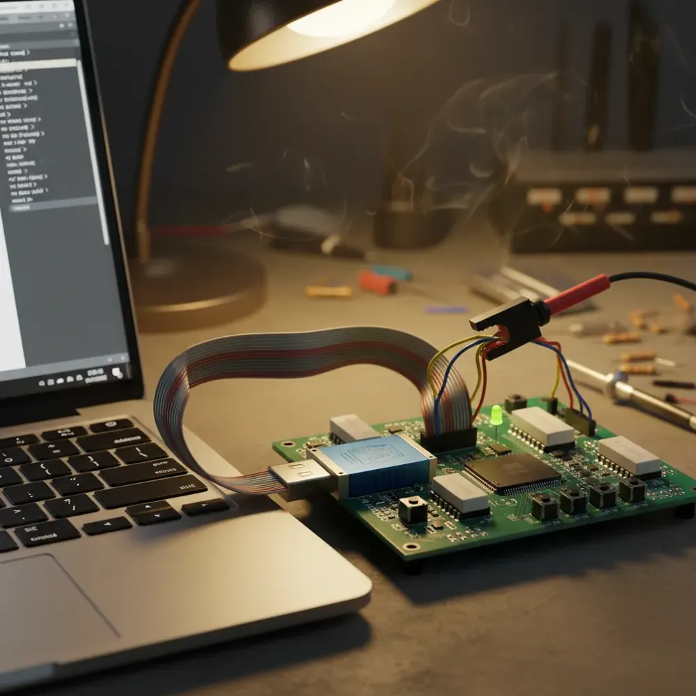
Programming I2C EEPROMs is one of the most common tasks for the Aardvark I2C/SPI Host Adapter. While Control Center Serial Software provides an interactive GUI for single read/write operations, its XML Batch Mode enables scripted, repeatable programming sequences that are essential for production workflows. This guide walks through programming an AT24C02 I2C EEPROM using batch mode.
Hardware Setup
The AT24C02 is a 256-byte (2 Kbit) I2C EEPROM with 8-byte page write capability. It is the EEPROM included on the I2C/SPI Activity Board.
Connections
| Aardvark Pin | Signal | AT24C02 Pin |
|---|---|---|
| Pin 4 | SCL | SCL (clock) |
| Pin 6 | SDA | SDA (data) |
| Pin 9 | GND | GND, A0, A1, A2, WP |
| Pin 10 | VCC | VCC (3.3V) |
The AT24C02’s address pins (A0, A1, A2) are tied to ground, setting the device’s I2C address to 0x50 (binary 1010000). The Write Protect (WP) pin is also grounded to enable write operations.
Control Center Configuration
Open Control Center Serial Software and configure the Aardvark:
1. Enable I2C: check the I2C checkbox in the adapter configuration.
2. Enable pullups: the Activity Board has on-board pullup resistors, but enabling the Aardvark’s internal pullups provides additional bus drive capability.
3. Enable target power: supplies 3.3V from the Aardvark to the Activity Board.
4. Set bitrate: 100 kHz is a safe starting point for EEPROM operations.
Writing with XML Batch Mode
Control Center’s Batch Mode executes a sequence of I2C/SPI commands defined in an XML file. For EEPROM programming, the XML script contains a series of I2C write commands, one per byte or page.
Batch Configuration
The XML batch script begins with an adapter configuration block:
```
```
Page Write Operation
Each write command sends a memory address byte followed by the data byte to the EEPROM’s I2C address:
```
00 AA
```
This writes the value 0xAA to EEPROM address 0x00. The first byte (0x00) is the word address inside the EEPROM; the second byte (0xAA) is the data.
To program the entire 256-byte EEPROM, the batch script contains 256 write commands, one per address. A 5 ms delay between writes ensures the EEPROM’s internal write cycle completes:
```
00 00
01 01
…
FF FF
```
This writes address 0x00 = 0x00, address 0x01 = 0x01, through address 0xFF = 0xFF, filling the EEPROM with its own address values for easy verification.
Sequential Read Operation
Reading back the EEPROM uses a two-step I2C sequence:
1. Set the address pointer: write the starting address to the EEPROM without sending a STOP condition.
2. Read the data: perform a read operation that retrieves bytes sequentially from the current address pointer.
In batch XML:
```
00
```
The `nostop=“1”` parameter on the write command generates an I2C Repeated Start instead of a Stop + Start sequence, which is required by most I2C EEPROMs for the “Set Address then Read” operation. The subsequent 256-byte read retrieves the entire EEPROM contents starting from address 0x00.
Verifying the Data
Compare the read-back data against the expected pattern. If you programmed address = data (0x00 at 0x00, 0x01 at 0x01, etc.), the read-back should produce an ascending sequence from 0x00 to 0xFF.
Moving to Production
For production programming workflows, the same operations can be automated through the Aardvark API in Python, C, or LabVIEW, reading firmware images from files and programming them into EEPROMs with pass/fail logging and serial number traceability. Flash Center Software also provides a GUI-based alternative that handles the entire read/program/verify cycle without writing any code.
GSAS Micro Systems provides the Aardvark alongside the I2C/SPI Activity Board for I2C EEPROM programming workshops and production test integration support across India.
Also appears in:
Interested in Total Phase tools?
Talk to our application engineers for personalized tool recommendations.
More from Total Phase
View all →
Aardvark vs Cheetah vs Promira: Total Phase Host Adapter Guide (India)
17 Jul · 6 min
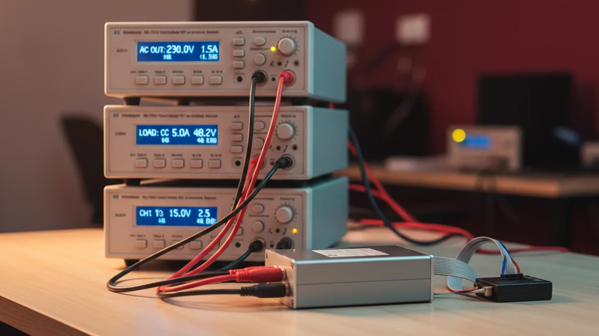
Automated EV Charger Test Bench in India: GW Instek AC Source, DC Load and Battery Emulator
6 Jun · 16 min
Best Logic Analyzer in India (2026): A Vendor-Neutral Buying Guide for Embedded Teams
5 Jun · 10 min
Capturing I²C/SPI Data to Train Edge AI: A Protocol-Analyzer Workflow for Indian Embedded Teams
4 Jun · 9 min

Emulating Processor Power for Thermal Testing: Why Constant Power
7 Oct · 7 min

CRPS and Rack Power Supply Testing: The Six Tests That Matter
7 Oct · 7 min