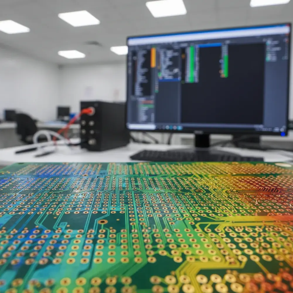
Every multilayer PCB fabricated today goes through electrochemical plating. Copper is deposited electrolytically to build up trace thickness, fill vias, and create conductive paths. When that deposition is uniform, the board works.
When it is not, you get opens in thin areas, shorts where copper overplates, impedance mismatches from uneven trace cross-sections, and reliability failures from stressed via barrels. The root cause is always the same: non-uniform current distribution during plating. Elsyca’s simulation tools, PCBBalance and PCBPlate, predict and correct this non-uniformity before a single panel enters the plating bath.
Why Copper Distribution Goes Wrong
Electrochemical plating follows a fundamental principle: current density is highest at points closest to the anode and at geometric protrusions, and lowest in recessed or shielded regions. On a PCB panel, this creates predictable problems.
Edges plate faster than centres. Panel edges sit closer to the anodes in a typical vertical plating cell. Edge traces can receive 30 to 50 percent more copper than centre traces. Isolated pads plate faster than dense arrays. An isolated pad surrounded by open copper acts as a current sink. A pad in a dense BGA array shares available current with neighbours, receiving less. Large pours plate faster than fine traces. A ground plane floods with current while a 75-micrometre signal trace, which needs copper the most, gets the least. Via aspect ratio matters. A deep, narrow via presents a long, resistive current path. The mouth plates well; the barrel midpoint receives much less copper, creating the “thin barrel” failure mode.
These effects compound on any modern design combining fine traces, wide pours, dense BGAs, and high-aspect-ratio vias.
Consequences of Non-Uniform Plating
Thin copper on fine traces. A 100-micrometre trace designed for 35-micrometre thickness receiving only 20 micrometres sees its resistance increase by 75 percent. Controlled-impedance traces shift outside specification. Overplating on edges. Excess copper can bridge adjacent traces, creating shorts. Overplated pads compromise solder mask adhesion. Thin via barrels. A via with a 12-micrometre barrel instead of the specified 25 micrometres passes electrical test but cracks under thermal cycling, creating intermittent opens that are nearly impossible to diagnose in the field.
Elsyca’s Simulation Approach
Elsyca models the complete electrochemical plating process from first principles, solving coupled equations for electric field distribution, ion transport, and reaction kinetics across the full three-dimensional geometry of the panel and plating cell.
PCBBalance: Design-Stage Copper Balancing
PCBBalance operates on Gerber or ODB++ layout data before fabrication. It analyses each layer’s copper pattern and predicts plating current distribution.
The output is a copper thickness map showing where the board will plate thick and thin. More importantly, PCBBalance recommends corrective actions.
Thieving pattern generation. Non-functional copper features (dots, lines, fills) are added to low-density areas to “steal” current from high-density areas, evening out distribution. PCBBalance generates these patterns automatically. Cross-layer balancing. In multilayer stackups, each inner layer’s copper pattern affects adjacent layers. PCBBalance analyses all layers together, ensuring balancing one does not destabilize another. Panel layout optimization. Board arrangement within a panel, rotation, spacing, border design, significantly affects uniformity. PCBBalance identifies the layout yielding the most uniform distribution.
PCBPlate: Process-Level Plating Simulation
PCBPlate models the plating cell itself, anode geometry, electrolyte flow, bath chemistry, and process parameters. While PCBBalance answers “will this design plate well?”, PCBPlate answers “how should I configure my process for this design?”
Via filling simulation. For via-in-pad HDI designs, PCBPlate predicts fill percentage as a function of plating chemistry and current profile, modelling the interaction between copper deposition and additive concentrations controlling bottom-up filling. Pulse plating optimization. PCBPlate simulates different pulse-reverse parameters, forward current, reverse current, duty cycle, frequency, to maximize uniformity without sacrificing throughput. Bath ageing effects. As baths age, additive concentrations drift and anode surfaces passivate. PCBPlate models these time-dependent effects, predicting when the bath will fall out of specification.
The Eurocircuits Validation
Elsyca’s accuracy has been validated by Eurocircuits, one of Europe’s leading PCB manufacturers. They compared simulated thickness maps from PCBBalance against actual cross-section measurements. Correlation was within 5 percent across the full panel, edges, centres, vias, fine traces, and copper pours, on standard production equipment, confirming the physics models are accurate enough for manufacturing use.
India’s PCB Manufacturing Context
India’s domestic PCB fabrication industry is at an inflection point. Government initiatives under Semicon India and NPE 2019 have attracted significant investment in new capacity. These facilities face a classic challenge: achieving first-time-right fabrication on complex designs.
The traditional approach, build a prototype, cross-section it, adjust parameters, rebuild, is slow and expensive. Elsyca simulation compresses this cycle. A new design can be analysed before the first panel is fabricated. Thieving patterns, panelization, and process parameters are optimized virtually. When the first physical panel is plated, it is already close to optimal.
As Indian electronics moves toward HDI boards with stacked microvias and substrate-like PCBs with 25-micrometre lines and spaces, plating uniformity requirements exceed what empirical process development can achieve. PCBPlate’s via filling simulation is critical here, predicting fill profiles for stacked microvia structures where underfill creates reliability risks and overfill creates planarity issues.
Getting Started with Elsyca in India
GSAS Micro Systems is the exclusive Indian representative for Elsyca’s complete simulation portfolio, including PCBBalance, PCBPlate, and surface finishing tools. We provide licensing, training, and ongoing technical support.
For PCB fabricators evaluating Elsyca, we offer a proof-of-concept: send us your most challenging design (Gerber files and stackup), and our team will run a PCBBalance analysis, delivering a copper thickness prediction and thieving pattern recommendation. Compare against your fabrication experience to evaluate simulation accuracy on your specific process.
Contact GSAS at gsasindia.com to initiate a proof-of-concept or discuss how Elsyca simulation integrates into your workflow.
Also appears in:
Interested in Elsyca tools?
Talk to our application engineers for personalized tool recommendations.
More from Elsyca
View all →
Elsyca PCBPlate: How Panel Plating Simulation Predicts Copper Thickness Before Fabrication
5 Apr · 6 min

Elsyca PlatingManager: Digital Twin Simulation for Industrial Electroplating Lines
4 Apr · 5 min

Copper Thieving for PCBs: Why Manual Methods Fail and How Simulation Fixes It
3 Apr · 5 min

Via Plating Reliability: Why Thin Barrels Fail and How Simulation Prevents It
2 Apr · 5 min

Emulating Processor Power for Thermal Testing: Why Constant Power
7 Oct · 7 min

CRPS and Rack Power Supply Testing: The Six Tests That Matter
7 Oct · 7 min