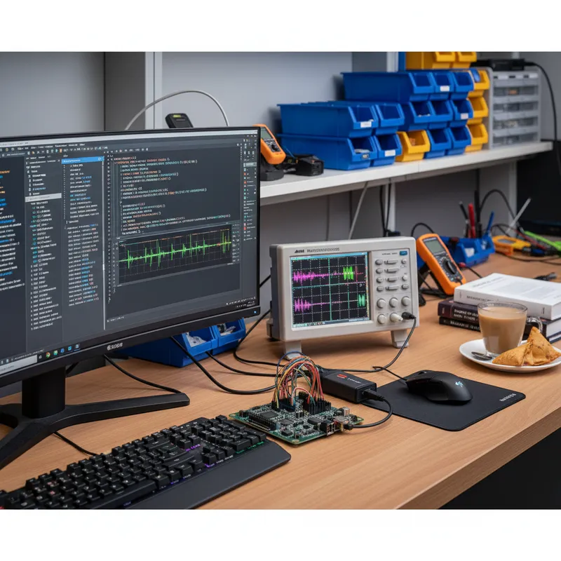
Selecting a QSPI flash looks simple on paper: pick a part with enough capacity, adequate speed, and a package that fits. In practice, SPI flash varies significantly across vendors in ways datasheets do not fully capture, command set quirks, timing margins under temperature, erase block granularity, and compatibility with your specific MCU’s QSPI controller. Choosing the wrong part means discovering issues late in development, when a board respin or flash qualification effort delays a product launch by months.
What Varies Across SPI Flash Parts
The SPI NOR flash market includes hundreds of variants from dozens of manufacturers. Key parameters that differ:
Speed and interface width. Single SPI, Dual SPI, Quad SPI (QSPI), and Octal SPI each double the data bus width. A part rated for “133 MHz Quad” delivers theoretical 66 MB/s throughput, but actual sustained speed depends on the MCU’s controller latency, dummy cycle requirements, and XIP (Execute-In-Place) support. Not all “QSPI” parts use the same quad-enable sequence.
Operating voltage. 3.3V parts are standard for industrial designs, but 1.8V is required for battery-powered applications where the MCU runs at lower voltages. Mixing 1.8V flash with a 3.3V MCU requires level shifters, adding cost and complexity.
Package. SO-8 (SOIC-8) is the most common and easiest to prototype. BGA offers smaller footprint but requires X-ray inspection. SON (DFN) packages provide a middle ground. Package choice affects not only layout but also which adapter boards you need for programming tools.
Endurance. Erase cycle counts range from 10,000 to 100,000+ depending on the part. For applications with frequent flash writes (data logging, configuration storage), this directly affects product lifetime.
SEGGER QSPI Flash Evaluator
SEGGER offers the QSPI Flash Evaluator board for flash qualification. It accepts SPI flash parts in multiple packages through adapter boards, SO-8, BGA, SON, DFN, and runs tests covering read speed, write speed, erase speed, command compatibility, and reliability.
The Evaluator tests hundreds of flash variants against a standardized benchmark, producing directly comparable results. Instead of breadboarding each candidate and writing custom test firmware, hardware teams get a controlled evaluation environment before committing to a design.
This is particularly valuable for qualifying second sources. A primary vendor’s part may work perfectly, but a second source with a nominally identical part number may differ in quad-enable bit behavior, status register layout, or erase suspend timing. The Evaluator catches these differences before production.
emFile NOR Flash Driver
SEGGER emFile includes a NOR flash driver optimized for SPI and QSPI flash. It handles sector mapping, wear leveling, and bad-block management, presenting flash as a standard file system. However, the driver must be configured for each flash part’s command set, sector size, and timing parameters.
Parts with non-standard quad-enable sequences, unusual status register layouts, or proprietary deep-sleep commands may require driver adjustments. Testing your chosen part with emFile early, ideally on the Evaluator, prevents late-stage integration issues.
J-Link and Flasher Flash Algorithms
J-Link debug probes and Flasher production programmers both depend on flash-specific algorithms for external QSPI flash programming. The algorithm must know the part’s command set, sector layout, and timing.
SEGGER maintains algorithms for a wide range of parts. The Evaluator’s results feed directly into algorithm validation. Verifying that a J-Link flash algorithm exists for your specific part avoids the scenario where development works fine with RAM download but production programming fails.
Evaluation Workflow
- Define requirements: capacity, speed, voltage, temperature range, package, endurance, second-source availability.
- Shortlist candidates: 3-5 parts from major vendors meeting specifications on paper.
- Evaluate on hardware: test each on the QSPI Flash Evaluator across operating temperature.
- Validate with emFile: run file system stress tests (write/read/delete cycles).
- Confirm programming: verify J-Link and Flasher algorithm support.
Flash Evaluation Tools in India
GSAS Micro Systems provides the SEGGER QSPI Flash Evaluator, emFile, J-Link, and Flasher with INR invoicing and local engineering support. Teams in Bengaluru, Chennai, Hyderabad, Pune, Mumbai, and Delhi NCR can access hands-on assistance for flash qualification, emFile integration, and production programming setup.
Also appears in:
Interested in SEGGER tools?
Talk to our application engineers for personalized tool recommendations.
More from SEGGER
View all →
Meet the GSAS Team at electronica India 2026, Stall H3.I45
15 Sept · 3 min
J-Link Is Now Validated by ST for StellarStudio
13 Sept · 2 min
An AI Agent That Drives the Debugger: SEGGER and Embedder Connect J-Link to the Loop
13 Sept · 6 min
SEGGER J-Link and J-Trace Now Support Andes Trace: Why This Matters for RISC-V
21 Jul · 6 min

Emulating Processor Power for Thermal Testing: Why Constant Power
7 Oct · 7 min

CRPS and Rack Power Supply Testing: The Six Tests That Matter
7 Oct · 7 min