SEGGER J-Link and J-Trace Now Support Andes Trace: Why This Matters for RISC-V
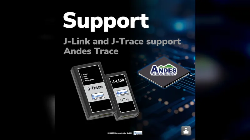
On July 10, 2026, SEGGER announced that its J-Link debug probes and J-Trace streaming trace probes now support Andes Trace from Andes Technology. One sentence in a news post, but it closes one of the last serious tooling gaps between the RISC-V world and the Arm world: professional, off-the-shelf instruction trace for one of the most widely deployed RISC-V core families.
Here is what Andes Trace actually is, and why probe support from SEGGER is a bigger deal than it sounds.
First, a primer: what instruction trace does
Instruction trace records the exact sequence of instructions a processor executes, in real time, without slowing the core down or halting it. A trace encoder inside the chip watches the core’s execution stream, compresses it (mostly by reporting only branches and discontinuities, since everything between two branches is knowable from the program image), and pushes the compressed stream to an on-chip buffer or out through dedicated trace pins.
The payoff: when firmware crashes once every three days in a way no breakpoint ever catches, trace lets you rewind and replay exactly what the core did in the moments before the fault. No printf instrumentation, no timing distortion, no “it stopped happening when I added logging.” The same execution record also drives on-target code coverage and performance profiling, which is why trace shows up in safety-critical workflows long before anything goes wrong.
Arm developers have had this for two decades through ETM and the mature probe ecosystem around it. RISC-V is younger: the trace standards were ratified much more recently, and probe support has been thin on the ground.
What Andes Trace is
RISC-V ended up with two ratified, complementary trace standards:
- E-Trace (Efficient Trace for RISC-V) defines the interface between the core (hart) and the trace encoder, plus a highly compressed, branch-based packet format. The compression is the point: only branches and deltas are reported, so more execution history fits through the same bandwidth, and multiple cores can be traced simultaneously.
- N-Trace defines a Nexus-based trace encoder and the output sink paths, how encoded trace actually leaves the system, whether into an on-chip buffer or out through trace pins to an external probe.
Andes Trace is a hybrid of the two. As SEGGER’s knowledge base describes it, Andes Trace combines the N-Trace standard with an E-Trace encoder. Concretely, Andes ships this as the AndesCore NCETRACE200 trace IP: an N-Trace compatible trace encoder, a timestamp generator, and a decoder, with a core interface that complies with the RISC-V Efficient Trace (E-Trace v2.x) instruction trace interface specification. It is designed to be non-intrusive and to scale across the entire Andes portfolio, from small low-power MCU cores up to high-performance out-of-order application processors.
In short: if a chip is built on Andes RISC-V IP with trace enabled, Andes Trace is how its execution history gets out.
What SEGGER announced
Both SEGGER probe families now speak Andes Trace:
- J-Link debug probes capture Andes Trace from the chip’s on-chip trace buffer: no extra pins needed, ideal for boards that never routed a trace connector.
- J-Trace streaming trace probes capture high-bandwidth trace off-chip through dedicated trace pins, for long, continuous recordings that an on-chip buffer could never hold.
SEGGER frames the capability exactly as trace veterans would want it framed: non-intrusive instruction tracing that lets developers analyze execution without affecting application behavior or timing, with visibility into real-time operation and timing-sensitive issues that instrumentation or halting would disturb.
Why this is a big deal
1. Andes is not a niche vendor. Andes Technology is a founding premier member of RISC-V International and one of the longest-established RISC-V CPU IP suppliers, with cores designed into SoCs across microcontrollers, wireless chips, storage controllers, and AI accelerators. When silicon built on Andes IP lands on your bench, the debug story for that chip is now a known quantity.
2. Trace was RISC-V’s credibility gap. Teams weighing RISC-V against Cortex-M for serious products kept hitting the same wall: “our current toolchain gives us streaming trace, coverage, and profiling; what is the RISC-V equivalent?” With mainstream probes now supporting Andes Trace, that answer no longer requires exotic, high-end tooling. The workflow embedded teams already run on Arm carries over.
3. One probe family across architectures. J-Link and J-Trace already cover Arm Cortex-M, Cortex-A/R, and RISC-V N-Trace targets. Andes Trace support means a team mixing Arm and Andes-based silicon across product lines keeps one set of probes, one flashing and debug workflow, and one set of muscle memory. No parallel toolchain to buy, learn, or maintain.
4. It unlocks certification-grade evidence on Andes targets. Instruction trace is the raw material for on-target code coverage and execution profiling, the kind of evidence functional-safety and medical programmes ask for. Bringing streaming trace to Andes-based devices puts those workflows within reach for RISC-V designs, the same way J-Trace PRO already does for safety-critical Arm projects.
What this means for Indian teams
India’s RISC-V momentum is real: indigenous processor programmes, a growing fabless startup scene, and design-services teams building RISC-V SoCs for global customers, a landscape we mapped in our guide to SEGGER tools in the Indian RISC-V ecosystem. Much of that commercial silicon is built on licensed core IP, and Andes is one of the names that comes up most often.
For an Indian team taping out or bringing up an Andes-based design, this announcement means the trace tooling question is answered before the evaluation starts: the same J-Trace PRO that handles streaming trace on Cortex-M handles the Andes parts too, and it is available locally, with INR invoicing and application-engineering support from GSAS in Bengaluru, Hyderabad, Chennai, Pune, Mumbai, and Delhi NCR.
If you are choosing between J-Link models for a RISC-V programme, start with our J-Link buyer’s guide, or talk to a GSAS engineer about a trace-capable evaluation setup for your target.
References
Also appears in:
Interested in SEGGER tools?
Talk to our application engineers for personalized tool recommendations.
More from SEGGER
View all →
Meet the GSAS Team at electronica India 2026, Stall H3.I45
15 Sept · 3 min
J-Link Is Now Validated by ST for StellarStudio
13 Sept · 2 min
An AI Agent That Drives the Debugger: SEGGER and Embedder Connect J-Link to the Loop
13 Sept · 6 min

Choosing a SEGGER Flasher: Standalone vs Gang vs Secure vs Portable
17 Jul · 7 min

Emulating Processor Power for Thermal Testing: Why Constant Power
7 Oct · 7 min

CRPS and Rack Power Supply Testing: The Six Tests That Matter
7 Oct · 7 min