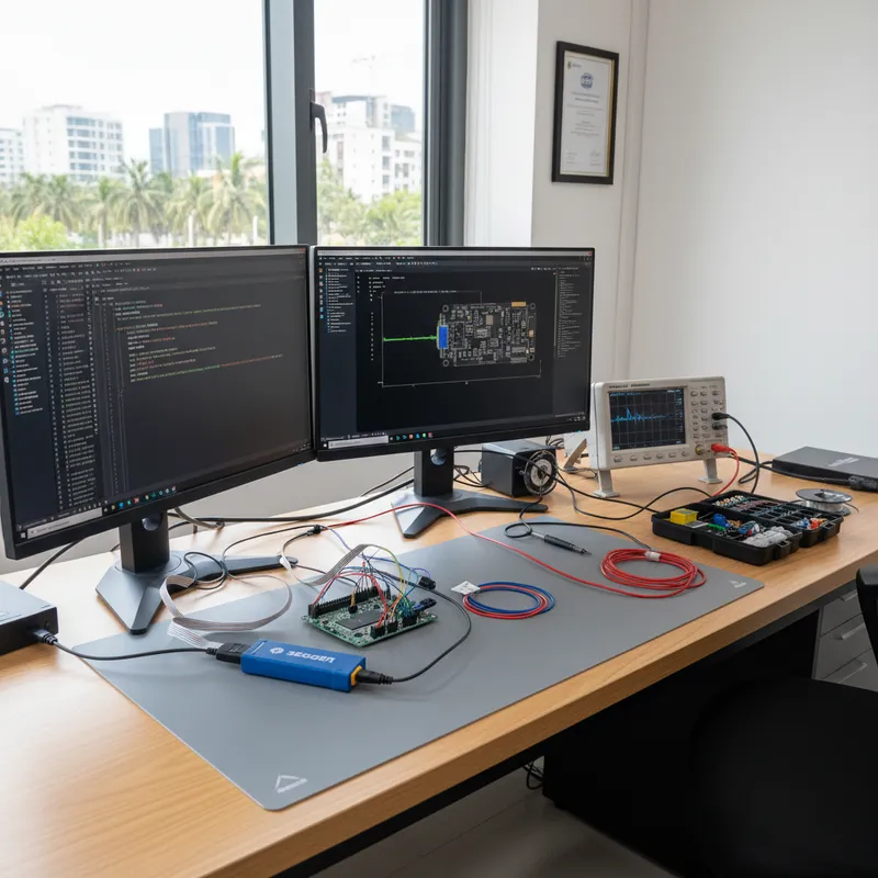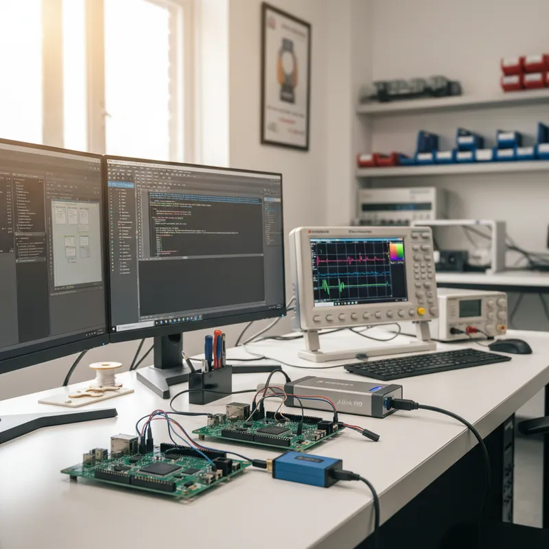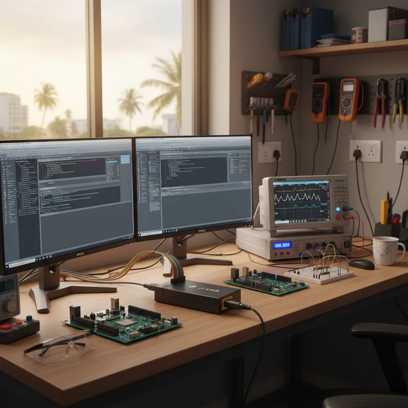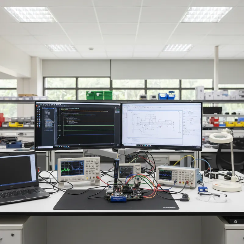
If you write commercial firmware in India for a living, you have almost certainly used a J-Link, or spent an afternoon wishing you had. With more than 500,000 J-Links shipped, SEGGER describes the J-Link debug probe family as probably the most popular debug probe for Arm cores and the de-facto standard. The family covers professional embedded debug, flash programming, and real-time trace across Arm Cortex-M, Cortex-R, Cortex-A, and RISC-V silicon. From a solo firmware engineer bringing up a Cortex-M0+ on the bench in Bengaluru to a production line in an EMS facility near Pune, one probe family covers the entire workflow.
This is the complete buyer’s guide to SEGGER J-Link for Indian engineering teams. By the end of it you will know exactly which J-Link model belongs on your bench, why commercial teams standardise on J-Link over CMSIS-DAP and vendor on-board probes, how RTT and SystemView change the way you debug RTOS workloads, when the Flasher family takes over for production, and how to buy J-Link in India through GSAS Micro Systems, an authorized SEGGER engineering partner in India.
What Is SEGGER J-Link?
J-Link is a family of USB-connected debug probes built by SEGGER Microcontroller GmbH, the German embedded software house best known for the embOS RTOS and the emFile/emNet/emUSB middleware stack. The probe sits between your host PC and the target MCU and speaks the full set of Arm and RISC-V debug interfaces, SWD (Serial Wire Debug), JTAG, cJTAG, SWO, and SEGGER’s own RTT (Real-Time Transfer) channel over the debug pins.
On the target side, the SEGGER device database spans tens of thousands of supported devices across every major Arm Cortex-M vendor, STM32 from STMicroelectronics, i.MX RT and Kinetis and LPC from NXP, RA and RX from Renesas, MSP432 and CC13xx/CC26xx from Texas Instruments, SAM from Microchip, nRF52/nRF53/nRF91 from Nordic Semiconductor, XMC and PSOC and AURIX from Infineon, EFM32/EFR32 from Silicon Labs, GD32 from GigaDevice, CH32V from WCH, ESP32 from Espressif, plus Cortex-A/R application cores and a growing list of RISC-V cores. One probe, one driver, one GDB Server, with free software and firmware updates from SEGGER.
On the host side J-Link plugs into every toolchain Indian teams actually use: Keil MDK, IAR Embedded Workbench, SEGGER Embedded Studio, Eclipse-based vendor IDEs (STM32CubeIDE, MCUXpresso, e² studio, Simplicity Studio, Code Composer Studio), CLI GDB workflows, VS Code with Cortex-Debug, and SEGGER’s own Ozone standalone GUI debugger. That combination, breadth of silicon, breadth of toolchain, and a single unified driver, is why so many commercial firmware teams standardise on J-Link.
The J-Link Model Lineup
There are more J-Link models than most first-time buyers expect, and the differences are real. Here is the commercial lineup in the order teams typically encounter it.
| Model | Interface | Download speed | Key differentiator | Best fit |
|---|---|---|---|---|
| J-Link BASE Compact | USB 2.0 Hi-Speed (USB-C) | Up to 1 MB/s | Entry-level commercial probe, full device database; Unlimited Flash Breakpoints, J-Flash and Ozone licences come via SEGGER’s paid BASE-to-PLUS upgrade | First commercial J-Link for a new engineer or cost-sensitive bench |
| J-Link BASE | USB 2.0 Hi-Speed | Up to 1 MB/s | Full-size 20-pin JTAG/SWD/cJTAG housing; same entry-level licence position as BASE Compact, with the standard 20-pin connector rather than the compact form factor | Benches standardised on 20-pin ribbon cabling |
| J-Link PLUS / PLUS Compact | USB 2.0 Hi-Speed | Up to 1 MB/s | Everyday workhorse; includes J-Flash, J-Flash SPI, Unlimited Flash Breakpoints, Ozone, monitor-mode debugging and RDI licences; pocketable Compact variant | Most Indian commercial firmware engineers |
| J-Link ULTRA | USB 2.0 Hi-Speed | Up to 4 MB/s | High-speed download and high-speed RTT, for large images, wireless logging, and log-heavy firmware | Throughput-bound benches, BLE/Wi-Fi logging, large OTA images |
| J-Link PRO | USB 2.0 Hi-Speed + Ethernet | Up to 4 MB/s | Ethernet interface for remote/shared debug (add a J-Link Isolator for galvanic isolation) | Shared lab racks, CI farms, remote debug over LAN/VPN |
| J-Link PRO PoE | USB 2.0 Hi-Speed + Ethernet with PoE | Up to 4 MB/s | Power and data over one Ethernet cable (802.3af), supplies up to 1 A to the target; Ozone, J-Flash, RTT and GDB Server licences included | Automated test racks where cable count drives reliability |
| J-Link WiFi | Wi-Fi + USB | Standard | Wireless host connection for hard-to-reach targets | Rotating jigs, thermal chambers, field prototypes |
| J-Link EDU / EDU Mini | USB 2.0 | Standard | Academic / non-commercial use only: same firmware, restricted license | Universities, hobby boards, student labs, not a commercial path |
| J-Trace PRO Cortex-M / Cortex-A/R / RISC-V | High-speed parallel trace | - | Full instruction trace (ETM/ETB), a different product family, not a J-Link upgrade | Functional safety evidence, hard-to-reproduce bugs, ISO 26262 / DO-178C / IEC 62304 |
A few clarifications that come up every week on the GSAS applications bench:
- BASE Compact vs PLUS Compact. Both are small, both are commercial, and both download at the same speed. PLUS adds the included licence bundle (J-Flash, Unlimited Flash Breakpoints, Ozone, monitor-mode debugging, RDI) and is the more commonly chosen workhorse.
- PLUS vs ULTRA. Both are USB 2.0 Hi-Speed. PLUS tops out around 1 MB/s of flash download; ULTRA pushes that to around 4 MB/s and also drives RTT at higher sustained rates. If you flash 2–4 MB images in a tight dev loop, ULTRA is worth it.
- PRO is not “ULTRA with Ethernet”. PRO’s real differentiator is the Ethernet interface for remote and shared debug over LAN or VPN, for distributed teams, CI farms, and shared lab racks; for custom automation it pairs with the separately licensed J-Link SDK. If your target is electrically hostile (EV power electronics, solar inverters, motor drives, industrial control), add a J-Link Isolator for target-side galvanic isolation or a USB Isolator for host-side protection, isolation is a separate accessory, not built into the PRO.
- J-Link EDU is not a cheap commercial probe. The licence is restricted to academic and non-commercial use. Any Indian team shipping a product should buy BASE Compact or above.
- J-Trace PRO is a different animal. J-Link gives you run control, flash, and RTT. J-Trace PRO adds true instruction trace via the ETM parallel trace port, the evidence artefact safety-critical teams need. If you are on a safety-critical programme, read the dedicated J-Trace PRO guide.
The J-Link EDU Mini Licence, Read This Before You Buy
SEGGER’s licence text for the J-Link EDU Mini is strict and unfamiliar to most procurement teams. SEGGER’s wording: “You may use the J-Link EDU Mini for non-profit educational purposes only.” It explicitly prohibits using the EDU Mini or its J-Link software “directly or indirectly for a profit organization, business purpose, or other commercial undertaking”, “directly or indirectly in any commercial environment (e.g. an office)”, “to develop, debug, program, or manufacture a commercial product (or parts thereof)”, or “to earn money or reasonably anticipate financial gain.” SEGGER adds: “A student using the J-Link EDU Mini directly or indirectly within a business or other profit organization (e.g. a company) is considered to be in violation of this agreement.”
In practical terms for India: if your engineering intern at a Bengaluru startup, your contractor in Pune, or a weekend side project you intend to monetise is using an EDU Mini, you are out of licence. EDU Mini is correct for university coursework, research labs and pure hobby bring-up. Once the work has any commercial intent, step up to J-Link BASE Compact or above.
The EDU Mini also has reduced specifications: 200 KB/s download, JTAG max 4 MHz, SWO max 4 MHz, and 1.8 V / 3.3 V target voltage. It is a bare-board design with a 9-pin 0.05 inch Samtec FTSH connector.
Why Indian Commercial Teams Standardise on J-Link
Indian commercial firmware teams rarely pick J-Link because of a single feature. They standardise on J-Link because four things compound in their favour over the life of a product.
Cross-silicon reuse. Indian product teams move across silicon families constantly. A medical device team in Chennai might start on an STM32F4, port to an STM32U5 for low power, then spin a variant on an nRF52840 for BLE. A two-wheeler EV team in Pune might prototype on an NXP i.MX RT1170, reuse the motor-control code on an Infineon AURIX, and sample a RISC-V GD32VF103 for the BMS. With J-Link, all of these share one probe, one driver, one device database, and one set of muscle memory. The alternative, a drawer full of vendor-specific on-board probes, each with its own firmware update cadence and IDE wiring, is what teams are actively moving away from.
Unlimited flash breakpoints. This is the single technical feature that converts senior engineers. Cortex-M cores have a small fixed number of hardware breakpoints, typically 4 or 6. On CMSIS-DAP and most vendor on-board probes, that is your hard ceiling. Set a seventh breakpoint and the previous ones start getting silently displaced, or the probe refuses to arm the breakpoint. J-Link patches flash on the fly to synthesise software breakpoints, giving you unlimited flash breakpoints on the J-Link PLUS and above (BASE owners can add the licence via SEGGER’s paid BASE-to-PLUS upgrade). If you have ever spent half a day debugging a weird symptom that turned out to be a breakpoint that never hit, you already know why this matters.
High-speed RTT. SEGGER’s Real-Time Transfer protocol streams data between target and host over the debug pins, using a small ring buffer in target RAM, with no UART required and no CPU halt. It is fast, MB/s sustained on ULTRA class probes, and non-intrusive, which means you can leave RTT logging enabled in BLE connection handling, real-time motor control loops, and interrupt service routines without distorting the timing you are trying to measure. This is the single biggest workflow change teams report after switching off of UART-based printf.
Ozone and the SEGGER tool ecosystem. J-Link PLUS and above include a licence for Ozone, SEGGER’s standalone GUI debugger (BASE owners can add it via the paid BASE-to-PLUS upgrade). Ozone takes any compiler’s ELF, GCC, Clang, Arm Compiler, IAR, SEGGER Compiler, and gives you full source-level debug, RTT viewer, SystemView integration, and power profiling. Paired with the SEGGER device database, tens of thousands of supported devices with free software and firmware updates, you get a long-term support story that vendor on-board probes cannot match.
J-Link vs CMSIS-DAP and Vendor Probes
This question comes up in every purchase conversation: why not just use the free probe already on the dev board?
CMSIS-DAP is the Arm-defined open debug protocol, and most modern Cortex-M evaluation boards ship with an on-board CMSIS-DAP probe. ST-Link is ST’s variant on every STM32 Discovery and Nucleo board. XDS110 is Texas Instruments’ equivalent on LaunchPads. NXP has LPC-Link2 and the MCU-Link family. Nordic has its own J-Link OB variant, a reduced-capability SEGGER OEM probe.
For hobby projects, bench evaluation, academic work, and first-touch bring-up of a single eval board, these on-board probes are genuinely fine. The gaps show up when you try to use them as your commercial development tool:
| Concern | Vendor / CMSIS-DAP probes | SEGGER J-Link (commercial) |
|---|---|---|
| Silicon coverage | One vendor, or whatever the on-board probe chip supports | Tens of thousands of supported devices across every major vendor and architecture |
| Flash breakpoints | Limited to the target’s hardware breakpoint count (typically 4–6) | Unlimited via flash patching from PLUS up (paid BASE-to-PLUS upgrade for BASE) |
| Real-time logging | UART or SWO, often halting or bandwidth-limited | RTT: MB/s, non-intrusive, no extra pins, no CPU halt |
| Standalone GUI debugger | Usually none, tied to a specific vendor IDE | Ozone licence included from PLUS up, works with any ELF, any compiler |
| Download speed | Adequate for small images | Up to 1 MB/s (PLUS) or 4 MB/s (ULTRA) |
| Ethernet / remote debug | Not available | J-Link PRO with Ethernet (add a J-Link Isolator for galvanic isolation) |
| Long-term device database | Vendor-specific, often lags new silicon | SEGGER-maintained, with free software and firmware updates |
| Toolchain portability | IDE-locked | Works across Keil MDK, IAR, Embedded Studio, Eclipse-based vendor IDEs, Ozone, VS Code |
For a team shipping one eval board, a vendor on-board probe is fine. For a team building a product line across three silicon vendors over five years, J-Link pays for itself in the first painful bug you would otherwise have spent a week on.
Which J-Link Model for Which Indian Team
The model lineup is wide on purpose. Here is the short answer for the most common Indian workflows.
| Your situation | Recommended model | Why |
|---|---|---|
| Bench dev / firmware engineer on a mixed STM32 + nRF52 workload | J-Link PLUS Compact | USB Hi-Speed, unlimited flash breakpoints, pocketable, fits any lab bag |
| High-throughput download, 2–4 MB images, BLE / Wi-Fi logging | J-Link ULTRA | Up to 4 MB/s download, high-speed RTT for log-heavy firmware |
| Powered test rig, EV traction, solar inverter, motor drive, industrial power | J-Link PRO + J-Link Isolator | Ethernet interface for the rack; add a target-side J-Link Isolator (or host-side USB Isolator) for galvanic isolation |
| CI farm / flash-and-test runners in a shared lab | J-Link PRO | Ethernet makes it rack-friendly; multiple probes on one host network |
| Rotating jig, thermal chamber, or awkward physical setup | J-Link WiFi | Wireless host connection where USB cabling is impractical |
| University / student project / non-commercial research | J-Link EDU or J-Link EDU Mini | Licence is academic / non-commercial only, do not use on shipping products |
| Functional safety evidence for ISO 26262 / DO-178C / IEC 62304 | J-Trace PRO (Cortex-M, Cortex-A/R, or RISC-V variant) | True instruction trace via ETM, evidence artefact safety auditors accept |
Two common mistakes we see in Indian procurement. First: teams buy J-Link BASE when they should be buying PLUS, the bundled licences (J-Flash, Unlimited Flash Breakpoints, Ozone, monitor-mode debugging) show up every day in the dev loop, and the delta is small compared to engineering time. Second: teams buy PRO for a normal dev bench “because it sounds like the highest-end one.” PRO is specifically for Ethernet/remote-debug and shared-lab scenarios; if your target is a 3.3 V eval board plugged into the same laptop, PLUS Compact or ULTRA is the right answer.
RTT and SystemView: The Killer Features
If you take one thing away from this guide, let it be this: the reason commercial teams move off vendor on-board probes and onto J-Link is rarely the probe itself. It is what the probe enables in the SEGGER software stack, specifically RTT and SystemView.
RTT (Real-Time Transfer) is a ring-buffer protocol that runs in a few hundred bytes of target RAM. Your firmware writes to the ring buffer with the same ergonomics as printf; the J-Link polls the ring buffer over the debug pins at MB/s rates and streams the data to the host. There is no UART pin to route on your PCB, no baud-rate negotiation, no interrupt overhead on the target, and crucially no CPU halt. You can log from inside a motor-control ISR, a BLE radio event, or a hard-real-time control loop without distorting the timing.
Teams that adopt RTT typically stop removing their debug logs for release builds. The old trade-off, “UART printf is too slow to leave in, so strip it before ship”, goes away. The full rationale, integration steps, and example code are in the RTT deep dive.
SystemView builds on RTT. It is a real-time RTOS visualiser: per-task CPU timing, context-switch traces, ISR latency, mutex and semaphore contention, event markers, and ELF-driven symbol resolution. Point it at an embOS, FreeRTOS, Zephyr, or Azure RTOS (ThreadX) build and you get a timeline view of what your scheduler is actually doing, down to the microsecond. For Indian medical-device and automotive teams that have to prove timing behaviour during design review, SystemView turns a heroic instrumentation effort into a few lines of initialisation code. The full workflow is in the SystemView RTOS profiling guide.
RTT and SystemView both require a J-Link. They are the reason a commercial J-Link pays for itself quickly.
Production Programming with the Flasher Family
Development and production are different problems, and the probe that is perfect for one is wrong for the other. J-Link is built around a host PC running GDB Server or Ozone, it assumes you have a developer in the loop. Once you are ready to program firmware onto finished units on a production line, that assumption breaks down.
This is where SEGGER’s Flasher family takes over. Flasher probes are standalone, they hold a firmware image in on-board storage, and a factory operator can trigger a program cycle without a PC attached. They are designed for the reliability, repeatability, and audit-trail requirements of an EMS production line.
- Flasher Compact: the entry-level standalone programmer; good for low-volume lines and field service kits
- Flasher PRO: the rackable workhorse for EMS production floors; Ethernet, SD card image storage, production-grade throughput
- Flasher ATE / Flasher ATE2: for multi-target ATE fixtures programming several boards in parallel on a panelised PCB
- Flasher Secure: for secure provisioning, encrypted firmware, and HSM-backed production flows where each unit must be cryptographically bound to a device identity
The exact decision, J-Flash on a J-Link vs standalone Flasher on the production line, is laid out in detail in the J-Flash vs Flasher decision guide. The short version: J-Link for dev and for low-volume internal production; a standalone Flasher as soon as you have an EMS partner running actual volume.
Buying J-Link in India
SEGGER J-Link is available in India through GSAS Micro Systems. GSAS is an authorized SEGGER engineering partner in India, and that word, “engineering partner”, is chosen deliberately. We do more than ship boxes.
What “authorized engineering partner” actually means for Indian teams:
- INR licensing under GST. Commercial J-Link purchases are invoiced in INR with full GST documentation, so the purchase order is raised in rupees and the import and customs handling sits with the partner rather than with your team.
- Local stock and fast dispatch. Common J-Link models, BASE Compact, PLUS, PLUS Compact, ULTRA, PRO, are held in GSAS stock for fast dispatch to engineering teams across India.
- On-site applications support. GSAS applications engineers help with first bring-up, target board layout review for trace, RTT integration into existing firmware, Ozone configuration, and CI/CD pipeline wiring with the J-Link Commander CLI.
- Production-line bring-up. When your project graduates from J-Link on a dev bench to Flasher on an EMS line, GSAS supports the transition, image build, PROJECT file setup, ATE integration, secure provisioning review.
- Full SEGGER middleware and RTOS portfolio. J-Link is the front door to the broader SEGGER catalogue. embOS (and embOS-Safe for ISO 26262), emFile, emNet, emSSL, emSSH, emModbus, emCrypt, emSecure, emUSB-Host, emUSB-Device, emWin, all available through GSAS with the same INR licensing and local support.
- Access to the full J-Link model lineup. Including J-Link PRO and J-Link PLUS, plus ULTRA, BASE Compact, WiFi, and the J-Trace PRO instruction trace family. If you need a model that isn’t in regular stock, GSAS can source it.
For India-specific silicon debug guides, STM32, TI MSP432 / CC13xx / CC26xx, GigaDevice and WCH CH32V, start with the STM32 complete guide, the TI MSP432 / CC13xx / CC26xx guide, and the GD32 / WCH CH32V guide. These walk through the exact device database entries, SWD wiring, and RTT configuration for each vendor family.
To evaluate J-Link for your team, request a demo, or start a commercial conversation, contact the SEGGER partner page on GSAS and the GSAS applications team will respond from the nearest office.
Further Reading
Canonical SEGGER documentation:
- SEGGER J-Link models overview, official model comparison and datasheets
- SEGGER J-Link knowledge base, configuration, troubleshooting, device-specific notes
GSAS India cross-links:
- SEGGER partner page, full SEGGER portfolio and the engineering partnership story
- J-Link PRO product page, Ethernet/remote-debug model for shared labs and CI farms
- J-Link PLUS product page, everyday commercial workhorse
- J-Link on STM32 in India, complete guide
- J-Link on TI MSP432 / CC13xx / CC26xx in India
- J-Link on GigaDevice GD32 and WCH CH32V in India
- SEGGER RTT, real-time transfer debugging
- SEGGER SystemView, RTOS profiling guide
- J-Flash vs Flasher, the Indian engineering decision
- J-Trace PRO for safety-critical teams in India
- J-Link Commander CLI for CI/CD pipelines in India
GSAS Micro Systems is an authorized SEGGER engineering partner in India. We support commercial firmware teams across Bengaluru, Chennai, Hyderabad, Delhi NCR, Mumbai, and Pune with local stock of the J-Link debug probe family, INR licensing under GST, on-site applications engineering, production-line bring-up with the Flasher family, and the complete SEGGER software stack, embOS, emFile, emNet, emSSL, emModbus, emCrypt, emSecure, emUSB, and emWin. If you are standardising your Indian engineering team on a single professional debug probe, J-Link is the conversation to have, and GSAS is how you buy it in India.
Also appears in:
Interested in SEGGER tools?
Talk to our application engineers for personalized tool recommendations.
More from SEGGER
View all →
Meet the GSAS Team at electronica India 2026, Stall H3.I45
15 Sept · 3 min
J-Link Is Now Validated by ST for StellarStudio
13 Sept · 2 min
An AI Agent That Drives the Debugger: SEGGER and Embedder Connect J-Link to the Loop
13 Sept · 6 min
SEGGER J-Link and J-Trace Now Support Andes Trace: Why This Matters for RISC-V
21 Jul · 6 min

Emulating Processor Power for Thermal Testing: Why Constant Power
7 Oct · 7 min

CRPS and Rack Power Supply Testing: The Six Tests That Matter
7 Oct · 7 min