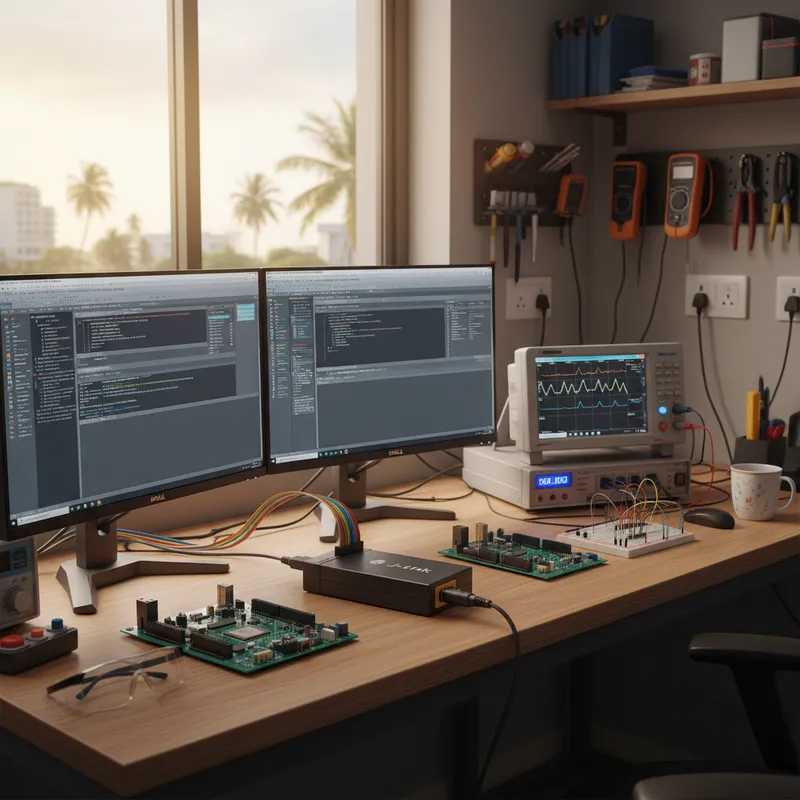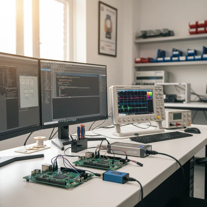
Every Indian STM32 engineer starts the same way. A Discovery or Nucleo board lands on the bench, USB cable goes in, the on-board ST-LINK enumerates, and within ten minutes the first blinky is running. That on-board ST-LINK is one of the best things STMicroelectronics does for the ecosystem, it is free, always present, and good enough to get a project off the ground. But there comes a moment, usually somewhere between the first prototype and the first customer pilot, where it stops being good enough. This post is about exactly that moment, and how to move your STM32 Discovery or Nucleo board from ST-LINK to a SEGGER J-Link PLUS or J-Link PRO without desoldering anything, rebuying your board, or rewriting your toolchain.
GSAS Micro Systems is an authorized engineering partner in India for SEGGER Microcontroller GmbH. Every J-Link model referenced here is available through GSAS in India with INR invoicing and GST documentation across Hyderabad, Chennai, Pune, Mumbai, and Delhi NCR.
What the on-board ST-LINK does well: and what it does not
The on-board ST-LINK on every STM32 Discovery and Nucleo board is remarkable for what it costs you: nothing. It speaks SWD to the target STM32, exposes a virtual COM port for printf-style debugging, offers drag-and-drop mass-storage flashing, and is supported out of the box by STM32CubeIDE. For the first hundred hours of any STM32 project, you will not miss anything.
What it does not do is what matters when your project becomes commercial. The ST-LINK firmware does not expose unlimited flash breakpoints, you are bound by the hardware breakpoint count of the Cortex-M core, which is typically six on Cortex-M4 and eight on Cortex-M7. The moment your debug session needs a ninth breakpoint, you have to start removing older ones by hand. ST-LINK does not implement SEGGER’s RTT (Real-Time Transfer) protocol natively. Community tooling can bridge RTT through OpenOCD with caveats, but for timing-critical instrumentation most teams end up wanting the native J-Link implementation. ST-LINK cannot drive Ozone, which is SEGGER’s performance timeline debugger, and it cannot drive SystemView, which is the tool you need when you want to prove an RTOS task has never missed its deadline. J-Flash, SEGGER’s production programmer that turns a debug image into a manufacturing-ready binary, also does not work with ST-LINK.
None of this means ST-LINK is a bad tool. It means ST-LINK is an evaluation and early-development tool. The minute a project crosses into commercial product engineering, the cost of not having flash breakpoints, RTT, Ozone, and SystemView starts to exceed the cost of a debug probe by an enormous margin.
Physically connecting J-Link to a Discovery or Nucleo board
The good news is that every modern STM32 Discovery and Nucleo board exposes a standard Cortex Debug connector, a 10-pin 1.27 mm pitch header with the SWD signals on well-known pins. SEGGER Application Note AN00021 (“Connecting J-Link to an STM32-Discovery board”) walks through this in detail, and the short version is that you need exactly four wires from the J-Link 20-pin connector to the Discovery board: VTref (so the J-Link senses the target voltage and level-shifts), SWDIO, SWCLK, and GND. Reset is optional but recommended.
On most STM32 Discovery boards, the on-board ST-LINK section sits at the top of the board and the target STM32 sits at the bottom, with a row of solder jumpers in between that connect the ST-LINK’s SWD lines to the target’s SWD lines. Those jumpers are usually labelled CN2 (or SB12/SB14, depending on board revision). To hand the debug interface over to an external J-Link, you do not need to desolder anything, you simply remove the two CN2 shorting caps. The target STM32’s SWD pins are then available on a separate SWD header (CN4 or similar, consult the Discovery user manual for your exact board).
On Nucleo boards the convention is slightly different: the SWD jumper block is typically called CN4, and you move the jumpers from the “ST-LINK” position to the “External” position. STMicroelectronics documents the exact jumper configuration in every Nucleo board user manual, the pattern is the same across F1, F4, F7, G0, G4, H7, L4, L5, U5, WB and WBA Nucleo boards.
Once the jumpers are removed or moved, a J-Link PLUS or J-Link PRO connected to the external SWD header has full, unshared control of the target MCU. The on-board ST-LINK is still powered by USB and the virtual COM port still works for UART printf, which is useful: you can keep the ST-LINK’s USB cable plugged in for power and serial, and use J-Link purely for debug.
What you gain the moment J-Link takes over
The first thing you notice is that flash breakpoints become unlimited. SEGGER’s J-Link firmware implements a patented flash-breakpoint mechanism that lets you set far more breakpoints than the Cortex-M core’s hardware breakpoint units support, because the debugger patches the flash on the fly. The Unlimited Flash Breakpoints license is included on J-Link PLUS and above; the entry-level J-Link BASE needs the paid BASE-to-PLUS upgrade to add it. For Indian teams working on control-loop code with dozens of conditional breakpoints during integration, this alone is worth the upgrade.
The second thing you gain is RTT (Real-Time Transfer). RTT is SEGGER’s high-speed, non-intrusive debug channel that moves printf and binary data between the target and the host over SWD with almost zero impact on target timing. In practice, a control loop that cannot afford to drop cycles for a UART write can keep logging continuously through RTT with minimal CPU overhead and without perturbing the timing. This is the difference between “the bug only happens in production and we cannot reproduce it in the lab” and “we captured the trace and here is the root cause”.
The third thing is the full SEGGER debug stack, Ozone (instruction trace, performance counters, code profiling timeline), SystemView (RTOS task and ISR visualisation), J-Flash (production programming images), and J-Run (automated test orchestration). Every one of these tools requires a J-Link to work, and together they are the difference between firmware engineering that ships products and firmware engineering that hopes products ship.
When should an Indian firmware team actually make the move?
Two practical rules of thumb that we see repeatedly at GSAS customer sites in Bengaluru, Hyderabad, Chennai, Pune, Mumbai, and Delhi NCR.
First rule: the moment your debug workflow routinely needs more than eight simultaneous breakpoints, you have outgrown ST-LINK. You will waste more engineering hours juggling breakpoints than a J-Link PLUS costs in the first week.
Second rule: the moment you spend a full 30-minute debug session chasing a bug you cannot reproduce twice, you need RTT and SystemView. Qualitative debug (“let me add a printf”) is finite. Instrumented debug (“let me capture a trace”) is infinite. Once a team crosses over to instrumented debug, they never go back.
There is a third rule for teams with production or CI ambitions: if you are flashing firmware images in a CI rack, or running hardware-in-the-loop tests on a test bench that lives in a separate room, you want J-Link PRO. J-Link PRO adds a 100 Mbit Ethernet interface alongside USB and a built-in web interface that makes it trivial to share one probe between multiple engineers over the LAN; for single-cable rack installations, the J-Link PRO PoE variant draws its power over Ethernet (802.3af). For an Indian EMS or ODM running a smoke-test rack on the factory floor, J-Link PRO is the correct default.
From prototype to product: the commercial upgrade path
To be clear about the upgrade path from the SEGGER lineup: when a project graduates from student work to commercial product engineering, the correct J-Link models are J-Link BASE, J-Link PLUS, J-Link PRO, and J-Link ULTRA. These are the commercial-licensed probes intended for paid product development. The J-Link EDU and J-Link EDU Mini are not a valid commercial upgrade path, they are licensed strictly for non-commercial educational use. If you are building a product you plan to sell, you need a commercial J-Link.
For most Indian STM32 teams leaving ST-LINK for the first time, J-Link PLUS is the natural starting point: USB, full SEGGER software stack, unlimited breakpoints, RTT, Ozone, SystemView. For teams that need shared access over Ethernet for a lab or test bench, J-Link PRO is the right step up. J-Link ULTRA exists for teams that specifically need the highest throughput: download speeds up to 4 MB/s in a compact USB-C housing.
Ordering through GSAS
Every SEGGER J-Link model referenced here is available through GSAS in India, serving Bengaluru, Hyderabad, Chennai, Pune, Mumbai, Delhi NCR, and Visakhapatnam. GSAS provides local application engineering support, INR invoicing, GST documentation, MSME and GeM procurement paths, and board-bring-up assistance for teams moving from ST-LINK to J-Link for the first time. For design-in evaluation, we can arrange a short-term loaner J-Link PRO so your team can prove out the workflow before procurement.
Further reading
- SEGGER Application Note AN00021, Connecting J-Link to an STM32-Discovery board: segger.com/downloads/application-notes/AN00021
- SEGGER J-Link PRO product page: segger.com/products/debug-probes/j-link/models/j-link-pro
- SEGGER RTT (Real-Time Transfer) overview: segger.com/products/debug-probes/j-link/technology/about-real-time-transfer
- GSAS, SEGGER J-Link PRO in India: /products/segger/j-link-pro
- GSAS, SEGGER J-Link PLUS in India: /products/segger/j-link-plus
- GSAS, SEGGER J-Link ULTRA in India: /products/segger/j-link-ultra
- GSAS, SEGGER J-Link STM32 complete guide: /blog/segger-j-link-stm32-india-complete-guide
- GSAS, SEGGER partner page: /partners/segger
Also appears in:
Interested in SEGGER tools?
Talk to our application engineers for personalized tool recommendations.
More from SEGGER
View all →
Meet the GSAS Team at electronica India 2026, Stall H3.I45
15 Sept · 3 min
J-Link Is Now Validated by ST for StellarStudio
13 Sept · 2 min
An AI Agent That Drives the Debugger: SEGGER and Embedder Connect J-Link to the Loop
13 Sept · 6 min
SEGGER J-Link and J-Trace Now Support Andes Trace: Why This Matters for RISC-V
21 Jul · 6 min

Emulating Processor Power for Thermal Testing: Why Constant Power
7 Oct · 7 min

CRPS and Rack Power Supply Testing: The Six Tests That Matter
7 Oct · 7 min