
Webinar
Predict Copper Distribution Before You Plate
This event has already taken place. Registration is closed, and any registration links below are kept for reference only. See upcoming GSAS events.
What’s covered
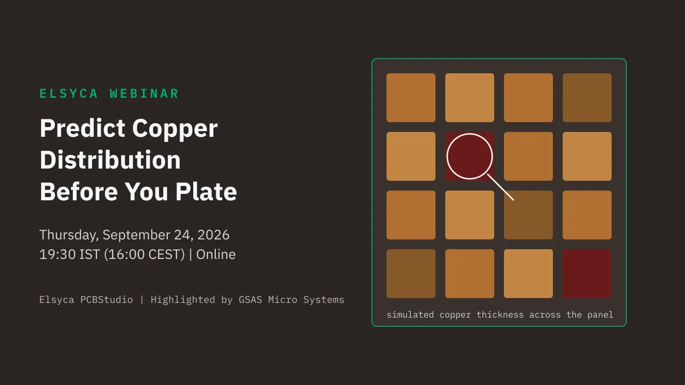
Predict Copper Distribution Before You Plate is an Elsyca webinar on Thursday, 24 September 2026 at 7:30 PM IST (4:00 PM CEST), presented by Reshmaa Selvakumar and Negin Madelat, on predicting and optimizing copper plating outcomes with Elsyca PCBStudio. Registration is open on Microsoft Teams; per the event page, anyone can view and join.
GSAS Micro Systems is highlighting Predict Copper Distribution Before You Plate, a webinar hosted by Elsyca and running 45 minutes on Microsoft Teams.
In Elsyca’s invitation framing, copper electroplating is one of the most sensitive steps in PCB manufacturing: small changes in panel layout, load, chemistry or rectifier settings can flip a board from in-spec to scrap, and uneven thickness, hotspots and under-plated regions stay invisible at the design stage until they surface on the line as cost, delays and reliability risk. The session addresses that gap with simulation, and the event page describes it as “walking through a real board from Gerber import to a production-ready, validated setup.”
What you will learn
Elsyca’s invitation lists these outcomes for the session, demonstrated in Elsyca PCBStudio:
- See finished copper thickness distribution across every board on the panel before production
- Automate copper balancing with what Elsyca describes as patented algorithms, generating optimized patterns fast
- Spot plating risks and thickness issues that standard DFM tools don’t show
- Reduce scrap and protect margins with fewer out-of-spec panels and less rework
- Deliver boards faster by preventing redesign loops and last-minute surprises
- Compare layout options on objective KPIs and enter production with confidence
Who should attend
The event page names six audiences for the session:
- PCB Manufacturing and Process Engineers
- OEM and PCB Layout Designers
- CAM and Pre-Production Engineers
- Quality, Yield and Reliability Leads
- Plating Line and Production Managers
- R&D and DFM Specialists
For Indian PCB fabricators, CAM teams and DFM specialists, the session runs live at 7:30 PM IST, so it fits after working hours without travel.
What is Elsyca PCBStudio?
Elsyca describes PCBStudio as its “suite for PCB plating simulation”, which includes two tools GSAS supports in India:
- Elsyca PCBBalance applies, in Elsyca’s words, “automated and optimized copper balancing to your PCB design and panel layout”. Elsyca calls it “The world’s only PCB DFM software”.
- Elsyca PCBPlate is described by Elsyca as a “graphical simulation platform for enhancing the plating performance” of PCB panel and pattern plating processes.
Speakers
Reshmaa Selvakumar
Business Developer - PCB | Elsyca
Negin Madelat
CAE Project Engineer | Elsyca
Per the speaker profiles on the event page, Negin Madelat holds a PhD in electrochemistry and surface engineering and brings more than 8 years of experience in the field.
Session details
| Detail | Information |
|---|---|
| Date | Thursday, 24 September 2026 |
| Time (India) | 7:30 PM to 8:15 PM IST |
| Time (Central Europe) | 4:00 PM CEST |
| Duration | 45 minutes |
| Format | Online live webinar (Microsoft Teams) |
| Host | Elsyca |
| Registration | Microsoft Teams event page |
Times sourced from the official Microsoft Teams event page: 16:00 CEST on 24 September 2026 is 7:30 PM IST.
Why GSAS is sharing this
GSAS Micro Systems has been an authorized Elsyca engineering partner since 2021, providing software licensing, application engineering, training and technical support for surface finishing simulation projects across automotive, aerospace and electronics teams, with India-wide support from Bengaluru, Hyderabad, Chennai, Pune, Mumbai and Delhi NCR.
Indian PCB fabrication and design teams sit close to this problem: plating uniformity decisions get made in the same programmes where GSAS already supports Elsyca electrochemical simulation work. If your team evaluates Elsyca PCBBalance or Elsyca PCBPlate, or you are scoping PCB plating simulation for an Indian site, talk to us.
Programme details, learning outcomes, audience list and speaker information are from Elsyca’s webinar invitation and the official Microsoft Teams event page. Elsyca hosts and organizes this webinar; GSAS Micro Systems is not the organizer.
More events
Other GSAS Events
Tradeshow
GSAS at embedded world India 2026
Tuesday, 17 November 2026
Webinar
Siemens EDA: What's New in Xpedition 2610
Thursday, 29 October 2026
Webinar
Siemens EDA: What's New in HyperLynx 2610
Thursday, 22 October 2026
Webinar
Siemens EDA: Master PartQuest for Faster PCB Designs in Xpedition
Tuesday, 29 September 2026