# UHDI PCBs: Why Indian OEMs Need to Prepare for Ultra-High Density Interconnect
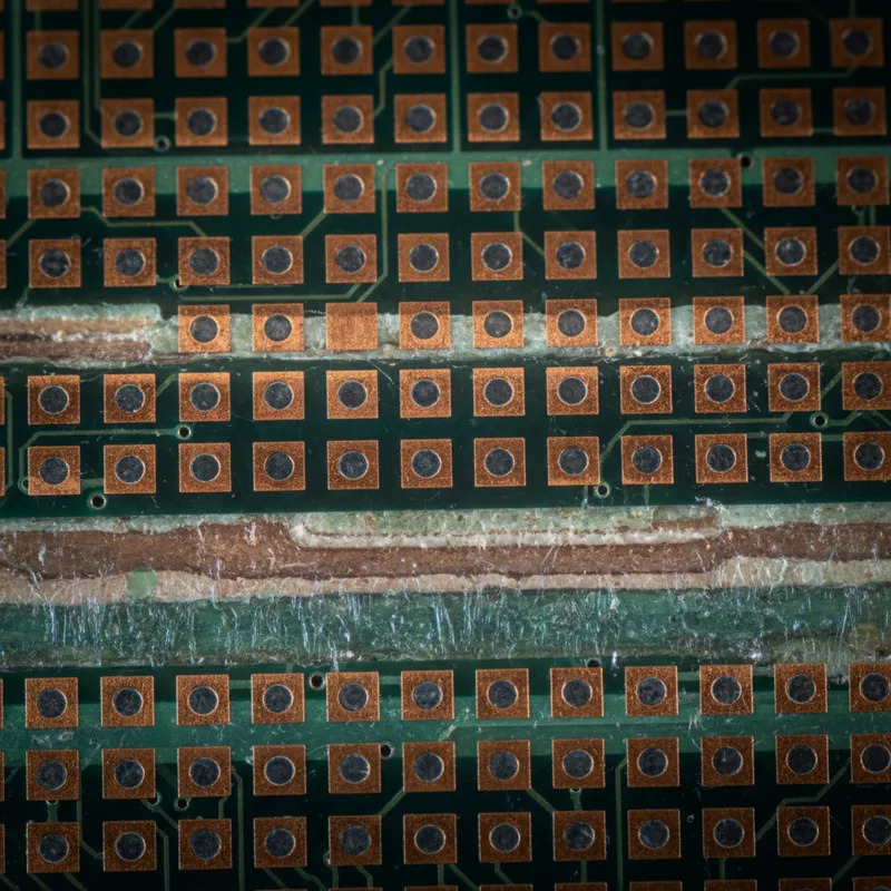
The printed circuit board industry classifies interconnect density into tiers, and each tier brings distinct design and manufacturing challenges. Standard PCBs handle trace widths above 100 micrometres with conventional processes. High Density Interconnect (HDI) boards push down to the 50-to-100 micrometre range using microvias and sequential lamination.
And then there is Ultra-High Density Interconnect, UHDI, where trace and space dimensions drop below 50 micrometres, and the manufacturing processes, materials, and design methodologies diverge fundamentally from anything most Indian PCB designers have encountered.
UHDI is not a distant future technology. It is being manufactured today for advanced packaging substrates, 5G millimetre-wave modules, and high-bandwidth memory interposers. For Indian OEMs and the emerging domestic semiconductor ecosystem, understanding UHDI design methodology is no longer optional, it is a strategic imperative.
What Defines UHDI
UHDI boards are characterised by several features that collectively push beyond the capabilities of conventional HDI manufacturing.
Sub-50 Micrometre Trace and Space. Where a typical HDI board might feature 75-micrometre traces with 75-micrometre spacing, UHDI designs routinely work at 25-micrometre or even 15-micrometre geometries. At these dimensions, the manufacturing process shifts from subtractive etching to semi-additive processes (SAP) or modified semi-additive processes (mSAP), where copper is built up through electroplating rather than etched away from a copper-clad laminate. Advanced Microvias. UHDI designs use laser-drilled microvias with diameters as small as 50 micrometres, stacked or staggered through multiple lamination cycles. Via-in-pad designs become the norm rather than the exception, and the reliability of stacked microvia structures requires careful attention to plating uniformity and thermal cycling performance. Sequential Lamination. UHDI boards are built up layer by layer through sequential lamination cycles. A 12-layer UHDI substrate might require four or five separate lamination cycles, each adding layers and vias. The cumulative registration accuracy across these cycles determines whether the final board meets design intent. Advanced Materials. Conventional FR-4 reaches its limits in UHDI applications. Low-loss laminates, modified epoxy systems, build-up films (ABF, Ajinomoto Build-up Film), and specialised dielectric materials become necessary to meet both the manufacturing process requirements and the electrical performance targets of UHDI designs.
Why UHDI Matters for India Now
The Semiconductor Packaging Connection
India’s semiconductor ambitions are no longer theoretical. With multiple fabrication and Assembly, Test, Marking, and Packaging (ATMP) facilities announced and under construction, India is positioning itself as a significant node in the global semiconductor supply chain. Advanced semiconductor packaging, chiplet architectures, 2.5D interposers, fan-out wafer-level packaging, requires UHDI substrate design capability.
The substrate that connects a chiplet package to the rest of the system is, fundamentally, a UHDI PCB. Indian companies involved in semiconductor packaging will need engineers who can design these substrates, and those engineers will need tools capable of handling UHDI constraints.
High-Bandwidth Memory and AI Hardware
The explosive growth of AI infrastructure is driving demand for high-bandwidth memory (HBM) and the interposer substrates that connect HBM stacks to processing dies. These interposers operate at UHDI geometries, and Indian companies designing AI accelerator boards or HBM-based systems need to understand the substrate design implications even if the interposer itself is manufactured offshore.
5G Millimetre-Wave Modules
India’s 5G rollout includes millimetre-wave (mmWave) spectrum allocations, and mmWave antenna-in-package modules require UHDI design techniques. The antenna elements, feed networks, and beamforming circuitry integrated into these modules operate at dimensions where UHDI processes are necessary to achieve the required electrical performance.
Miniaturisation Pressure Across Sectors
Indian OEMs in wearable medical devices, compact industrial IoT sensors, and consumer electronics face relentless miniaturisation pressure. As component packages shrink and pin counts increase, the PCB interconnect must densify correspondingly. UHDI capabilities give Indian designers the tools to meet these packaging challenges.
Design Tool Requirements for UHDI
UHDI design is not simply “smaller HDI design.” The design tool requirements shift in several fundamental ways that affect tool selection and workflow configuration.
Constraint Management at Manufacturing Limits
At UHDI geometries, the design rules are not just tighter, they interact in ways that do not occur at conventional dimensions. Etch compensation, copper distribution, microvia aspect ratios, and sequential lamination registration all impose constraints that must be managed simultaneously. The design tool must support manufacturing-aware constraint systems that account for these interactions rather than treating each rule independently.
Xpedition’s constraint management system handles UHDI-class rules with the granularity required, per-layer clearances, microvia stack rules, copper balance constraints, and technology-specific DRC rules that reflect the actual manufacturing process rather than idealised geometries.
DRC at the Limits
Design rule checking for UHDI boards must account for manufacturing variability at scales where conventional DRC margins are insufficient. A 25-micrometre trace with a 10-percent manufacturing tolerance means the actual trace could be as narrow as 22.5 micrometres, and the DRC system needs to validate that the design is manufacturable across the expected process window, not just at nominal dimensions.
Via Structure Management
UHDI designs require sophisticated via structure management, stacked microvias, staggered microvias, via-in-pad with plated-over caps, and back-drilled vias for high-speed signals. The design tool must support these structures as first-class objects with their own constraint rules, not as workarounds assembled from primitive geometric shapes.
Valor NPI: Manufacturing Awareness for UHDI
Designing a UHDI board that passes DRC is necessary but not sufficient. The design must also be manufacturable with the specific processes and capabilities of the target fabricator. This is where Valor NPI becomes critical for UHDI design workflows.
Valor NPI performs Design for Manufacturability (DFM) analysis against actual manufacturing capability profiles. For UHDI designs, this means validating that the trace geometries are achievable with the fabricator’s SAP or mSAP process, that the microvia structures are within the fabricator’s laser drilling and plating capabilities, and that the sequential lamination build-up is compatible with the fabricator’s registration and lamination equipment.
For Indian design teams working with advanced fabricators, whether domestic facilities ramping UHDI capability or established offshore partners, Valor NPI provides the manufacturing awareness that prevents designs from arriving at the fab only to be flagged as unmanufacturable.
Innovator3D: Advanced Packaging Substrates
For designs that cross the boundary between PCB and semiconductor packaging, interposers, substrates for chiplet architectures, fan-out packages, Siemens EDA’s Innovator3D provides a design environment specifically tailored to advanced packaging substrate design. This tool addresses the unique requirements of package substrate design: redistribution layers, bump patterns, through-silicon via planning, and die-to-substrate co-design.
Indian companies entering the ATMP space will find Innovator3D essential for substrate design work that exceeds the scope of conventional PCB layout tools, even UHDI-capable ones.
Material Considerations for Indian Teams
UHDI design forces a deeper engagement with materials than most Indian PCB designers have needed historically. Several material considerations are particularly relevant.
Low-Loss Laminates. At UHDI geometries and the frequencies associated with high-speed interfaces, dielectric loss becomes a significant design factor. Low-Dk (dielectric constant) and low-Df (dissipation factor) laminates are standard in UHDI applications. Indian designers need to understand how material properties affect impedance, insertion loss, and signal integrity at UHDI dimensions. Build-Up Films. ABF and similar build-up film materials are the dielectric layers in sequential lamination UHDI processes. These materials have different thermal, mechanical, and electrical properties compared to conventional prepreg, and the design must account for these differences in stackup design and reliability analysis. Modified FR-4 Systems. For UHDI designs that do not require the lowest-loss materials, modified FR-4 systems with improved dimensional stability and finer glass weave can bridge the gap between conventional laminates and specialised UHDI materials. Understanding where modified FR-4 is adequate and where specialised materials are necessary is a key engineering decision.
Z Planner Enterprise, Siemens EDA’s stackup design tool, supports the material libraries and modelling capabilities needed to design UHDI stackups with accurate impedance predictions across these diverse material systems.
Preparing for the UHDI Future
Indian OEMs do not need to be designing UHDI boards today to benefit from UHDI preparation. The preparation path involves several practical steps.
Skill Development. Understanding UHDI design principles, even if current designs are at conventional HDI densities, positions engineering teams to scale their capabilities as product requirements evolve. Training on constraint management, DFM analysis, and stackup design for fine-geometry boards builds foundational knowledge. Tool Readiness. Ensuring that your design tool chain can handle UHDI constraints when needed means you are not scrambling for new tools when a product requirement demands finer geometries. Xpedition, Valor NPI, and Z Planner Enterprise are UHDI-ready today. Fabricator Relationships. Building relationships with fabricators who have UHDI capability, and understanding their specific process constraints, is essential groundwork. Valor NPI’s fabricator-specific DFM profiles formalise these relationships into the design workflow. Material Knowledge. Developing familiarity with advanced laminate systems, build-up films, and their design implications before they are needed on a production schedule eliminates a steep learning curve at the worst possible time.
The Indian UHDI Opportunity
India’s simultaneous push into semiconductor packaging, 5G infrastructure, AI hardware, and advanced electronics manufacturing creates a unique convergence that will drive UHDI adoption. Indian engineers who develop UHDI design expertise now will be positioned at the centre of the country’s most strategically important technology initiatives.
The design tool chain, the manufacturing awareness, and the material knowledge required for UHDI are all available today. What is needed is the deliberate decision to invest in these capabilities before they become urgent.
Ready to prepare your design team for UHDI? Contact GSAS Micro Systems for a UHDI design methodology consultation. Our engineers will assess your current design capabilities, identify the gaps between your present workflows and UHDI requirements, and develop a readiness plan tailored to your product roadmap and manufacturing strategy. GSAS Micro Systems: an authorised Siemens EDA partner. Bengaluru | Pune | Noida gsasindia.com | info@gsasindia.com
Also appears in:
Interested in Siemens EDA tools?
Talk to our application engineers for personalized tool recommendations.
More from Siemens EDA
View all →
India's EDA Moment: Why Design Tool Demand Is Growing, and the Engineering Careers It Creates
21 Sept · 9 min

AI and Complexity Are Redrawing EDA: Siemens on the Trillion-Transistor Era
13 Sept · 6 min

Calibre Vision AI: Bringing Order to DRC Debug at Advanced Nodes
24 Aug · 4 min

Siemens EDA EBS Expert Series: 6 Free PCB Design Webinars (Jul-Aug 2026)
20 Jul · 8 min

Emulating Processor Power for Thermal Testing: Why Constant Power
7 Oct · 7 min

CRPS and Rack Power Supply Testing: The Six Tests That Matter
7 Oct · 7 min