# Etch Effects and Copper Distribution: What Every Indian PCB Designer Should Know
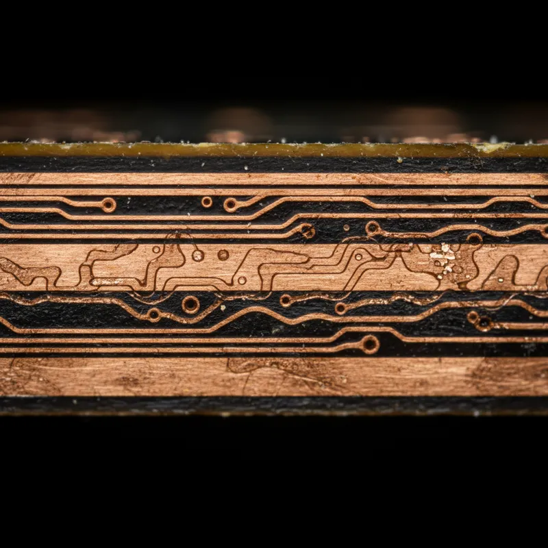
There is a fundamental disconnect in PCB design that most engineers encounter only when a board fails to meet impedance targets or when a fabricator flags a manufacturability concern. The disconnect is this: the traces on your screen are not the traces on your board. The clean, perfectly rectangular copper conductors rendered in your layout tool become trapezoidal cross-sections with width variations after the etching process.
And the uniformity of your copper distribution affects not just the traces themselves but the plating, etching, and impedance of every other feature on the same layer.
For Indian PCB designers working with domestic fabricators, where process controls may vary significantly between facilities, understanding etch effects and copper distribution is not an academic exercise. It is the difference between a board that meets specifications on the first fabrication run and one that requires multiple respins to achieve target impedance.
The Hidden Problem: Traces Are Not What They Seem
When you draw a 100-micrometre trace in your layout tool, you are defining the intended width at the design level. What the fabricator produces is determined by the etching process, and etching is inherently an imperfect process.
In subtractive etching, the dominant process for conventional PCB manufacturing, the fabricator starts with a copper-clad laminate and removes copper everywhere except where traces, pads, and planes should remain. The etchant (typically cupric chloride or alkaline ammonia-based solutions) attacks the copper chemically, dissolving it from the exposed surfaces.
The problem is that the etchant does not only remove copper vertically. It also removes copper laterally, undercutting beneath the etch resist that defines the trace pattern. This lateral etching means that the finished trace is narrower than the resist pattern, and the amount of undercut depends on the copper thickness, the etch chemistry, the etch time, the conveyor speed, and the age and concentration of the etch bath.
For a typical inner layer with 35-micrometre (1 oz) copper, the total undercut might be 15 to 25 micrometres per side. A trace designed at 100 micrometres might emerge from the etch process at 50 to 70 micrometres, a 30 to 50 percent reduction in width. At tighter geometries, this undercut represents an even larger fraction of the intended width.
Etch Compensation: The Fabricator’s Adjustment
Fabricators account for etch undercut by applying etch compensation, widening the artwork pattern so that after etching, the resulting trace width matches the designer’s intent. If the expected undercut is 20 micrometres per side, the fabricator widens the artwork by 20 micrometres on each side, producing a resist pattern that is 40 micrometres wider than the target trace width.
This compensation is not applied uniformly across the board. Different regions of the panel may etch at slightly different rates due to spray nozzle distribution, etch bath flow patterns, and panel position in the etching equipment. The fabricator applies compensation based on their process characterisation, but some variation is inevitable.
For Indian designers working with fabricators across different capability tiers, understanding etch compensation is critical. A fabricator in one facility may have tightly controlled etch compensation with minimal variation, while another facility may have wider process spreads that affect impedance consistency. Knowing your fabricator’s etch compensation practices, and their typical variation, allows you to set realistic impedance tolerances and identify potential manufacturing risks before the board is built.
Trapezoidal Cross-Sections: The Impedance Impact
The most significant consequence of the etch process for signal integrity is the trapezoidal cross-section of etched traces. Because the etchant attacks copper from the top surface and works downward, the top of the trace is exposed to the etchant longer than the bottom. The result is a trace that is wider at the base (near the laminate) and narrower at the top, a trapezoid rather than a rectangle.
This trapezoidal profile has direct implications for impedance and insertion loss. The effective width of a trapezoidal trace is less than the base width but more than the top width, and the impedance depends on this effective width along with the dielectric thickness and dielectric constant. A signal integrity simulation that models traces as ideal rectangles will produce impedance predictions that are systematically offset from the actual manufactured board.
The etch angle, the angle of the trapezoid sidewalls relative to vertical, depends on the copper thickness and the etch process. Thinner copper produces steeper sidewalls (closer to rectangular), while thicker copper produces more pronounced trapezoids. For a typical outer layer with 35-micrometre copper, the etch angle might be 60 to 75 degrees from horizontal, producing a top width that is 20 to 40 micrometres narrower than the base width.
At multi-gigabit data rates, where impedance tolerances of plus or minus five percent are common requirements, ignoring the trapezoidal cross-section can account for the entire tolerance budget before any other manufacturing variation is considered.
Inner Layer Versus Outer Layer Etch Characteristics
The etch process differs significantly between inner layers and outer layers, and this difference affects impedance, trace width control, and manufacturing yield in ways that Indian designers should account for in their stackup and routing decisions.
Inner Layers. Inner layers use a pattern-and-etch process on uniform foil thickness (typically 17.5 or 35 micrometres). The etch process is relatively consistent, etch compensation is well-characterised, and trace width control is generally tighter than on outer layers. Outer Layers. Outer layers undergo electroplating before etching, increasing total copper thickness to 50-70 micrometres. This thicker copper produces more pronounced trapezoidal profiles and wider process variation. The plating thickness itself is not perfectly uniform across the panel, introducing another source of impedance variation.
For impedance-critical designs, Indian designers should route critical high-speed signals on inner layers where etch control is tighter, reserving outer layers for less impedance-sensitive connections and power distribution.
Copper Distribution: The Plating and Etching Equaliser
Copper distribution, how evenly copper is distributed across each layer of the board, affects both the plating process and the etching process, creating a cascade of manufacturing effects that many designers overlook.
Plating Uniformity. During electroplating, copper deposition rate is proportional to current density. Sparse areas plate thicker; dense areas plate thinner. This non-uniformity translates directly to trace width and impedance variation. Adding copper balancing features, thieving patterns, copper fills, and equalisation pads, in sparse areas improves plating uniformity and impedance consistency. Etch Uniformity. Regions with more exposed copper consume more etchant locally, affecting etch rates in adjacent regions. Uniform copper distribution produces more consistent trace widths. For Indian fabricators using older etching equipment with less sophisticated spray distribution, copper balancing becomes even more important.
Valor NPI: Catching Etch-Related Issues Before Fabrication
Valor NPI’s DFM analysis includes checks specifically targeting etch-related manufacturing issues. These checks evaluate the design against the manufacturing capability of the target fabricator, flagging issues that will cause problems during the etch process.
Acid Trap Detection. Acute-angle trace junctions create acid traps where etchant is retained after the main etch cycle, causing over-etching at the junction. Valor NPI identifies these geometries and flags them for correction. Copper Balance Analysis. Valor NPI analyses copper distribution across each layer and identifies regions where the imbalance will affect plating uniformity or etch consistency. The analysis quantifies the imbalance and identifies the specific areas where copper balancing features are needed. Minimum Trace and Space Verification. Beyond simple DRC, Valor NPI verifies that trace widths and spaces, after accounting for the fabricator’s etch compensation and process variation, will meet the design intent. A trace that passes DRC at nominal dimensions might fail manufacturing verification when the fabricator’s process variation is factored in. Annular Ring After Etch. The etch process reduces pad sizes along with trace widths. Valor NPI verifies that annular rings around plated through-holes and vias remain adequate after etch compensation is applied, preventing breakout conditions that would not be caught by DRC alone.
HyperLynx: Modelling Real Etch Profiles
HyperLynx supports trapezoidal cross-section modelling for transmission line impedance and loss calculations. Rather than assuming ideal rectangular trace profiles, designers can specify the etch angle and model the actual manufactured cross-section. For differential pairs, the trapezoidal profile affects the coupling coefficient and differential impedance, modelling both traces with realistic etch profiles produces impedance predictions that correlate closely with TDR measurements on fabricated boards.
Z Planner: Stackup Design with Etch Awareness
Z Planner Enterprise supports etch-aware stackup design, accounting for etch effects when selecting trace widths and dielectric thicknesses. By entering the specific etch parameters of your target fabricator, etch angle, typical undercut, process variation, Z Planner produces stackup recommendations tailored to the actual manufacturing process rather than idealised geometries.
Working with Indian Fabricators
Indian PCB fabricators span a wide range of capabilities, from facilities running older equipment with manual process controls to modern factories with automated etch lines and statistical process control. Understanding where your fabricator sits on this spectrum, and how that positioning affects etch compensation, trace width control, and impedance consistency, is a practical necessity for Indian design teams.
Request Etch Process Data. Ask your fabricator for their typical etch undercut per side for the copper weights you use. Ask for their etch angle characterisation data. Ask for their process capability indices for trace width control. Fabricators who can provide this data have characterised their process; those who cannot may have less predictable manufacturing outcomes. Design for the Process Window. Set trace widths and spaces that give the fabricator margin within their process window. A design that requires every parameter to be at the edge of the fabricator’s capability is a design that will have yield problems. Use Copper Balancing. Add copper thieving and balancing features to equalise copper distribution across each layer. This is one of the simplest and most effective steps a designer can take to improve manufacturing consistency with any fabricator.
Ready to improve the manufacturability of your PCB designs? Contact GSAS Micro Systems for PCB manufacturability training. Our engineers will help your team understand etch effects, copper distribution, and DFM best practices tailored to the fabricators you work with, ensuring that your designs manufacture correctly on the first build. GSAS Micro Systems: an authorised Siemens EDA partner. Bengaluru | Pune | Noida gsasindia.com | info@gsasindia.com
Also appears in:
Interested in Siemens EDA tools?
Talk to our application engineers for personalized tool recommendations.
More from Siemens EDA
View all →
India's EDA Moment: Why Design Tool Demand Is Growing, and the Engineering Careers It Creates
21 Sept · 9 min

AI and Complexity Are Redrawing EDA: Siemens on the Trillion-Transistor Era
13 Sept · 6 min

Calibre Vision AI: Bringing Order to DRC Debug at Advanced Nodes
24 Aug · 4 min

Siemens EDA EBS Expert Series: 6 Free PCB Design Webinars (Jul-Aug 2026)
20 Jul · 8 min

Emulating Processor Power for Thermal Testing: Why Constant Power
7 Oct · 7 min

CRPS and Rack Power Supply Testing: The Six Tests That Matter
7 Oct · 7 min