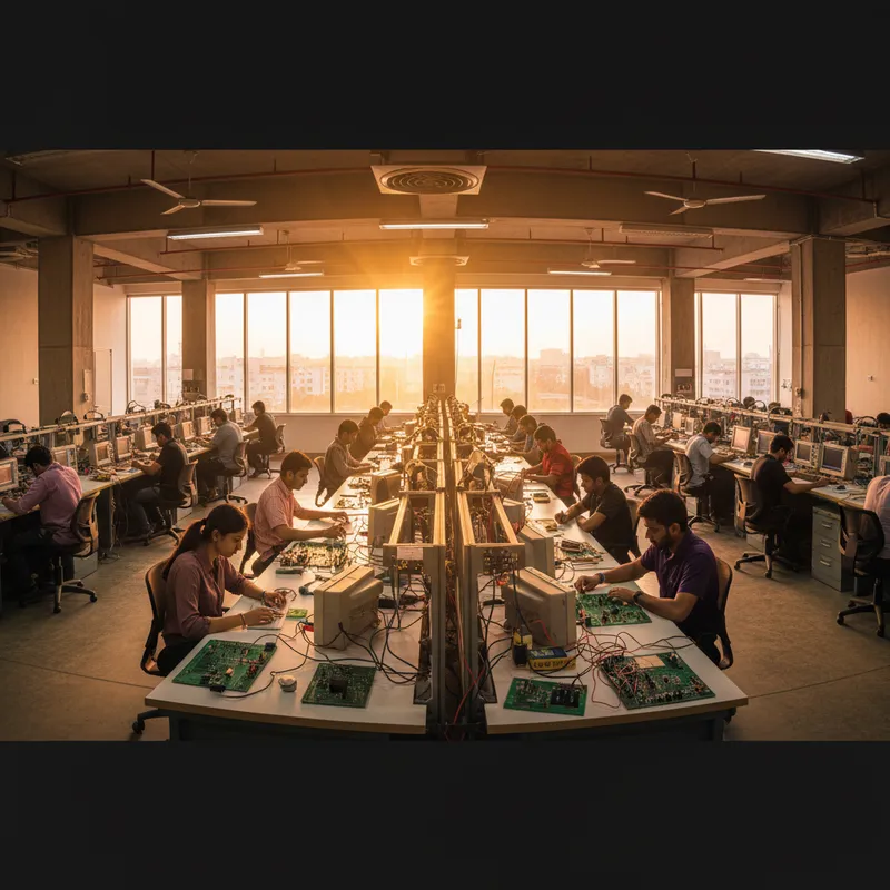
India’s PCB manufacturing sector is undergoing its most significant expansion in decades. Government incentives, Production Linked Incentive (PLI) schemes for electronics manufacturing, Make in India policy directives, and semiconductor-related investment programmes, are channelling capital into domestic PCB fabrication capacity. New facilities are being built, existing facilities are upgrading, and the ambition is to move India from a low-volume, low-complexity PCB fabrication base to a competitive producer of multilayer, HDI, and high-reliability boards.
This ambition is technically achievable. But the fabrication capabilities that India is investing in, 12+ layer multilayer, HDI with sequential lamination, controlled impedance, high-aspect-ratio vias, demand process control sophistication that scales non-linearly with board complexity. Electroplating, in particular, becomes a yield-critical process step as board complexity increases.
The Complexity Curve
A 4-layer standard-tolerance board is relatively forgiving of plating variation. The traces are wide, the vias have low aspect ratios, and the impedance tolerance bands are generous. A 30% variation in copper thickness across the panel is manageable.
A 12-layer controlled-impedance board with 100-micrometre traces, 10:1 aspect ratio vias, and +/- 7% impedance tolerance is not. At these specifications, a 30% plating variation means some traces are below minimum thickness (reliability risk), some are above maximum (impedance excursion), and some vias have thin barrels (thermal cycling failure risk). The reject rate climbs, and the fabricator’s cost per good board increases.
An HDI board with microvias, stacked via structures, and fine-pitch features pushes the plating challenge further. Copper filling of microvias, uniform plating on fine traces, and panel-level thickness control must all be achieved simultaneously, within a process window that shrinks as features get smaller.
Where Indian Fabricators Are Today
The majority of Indian PCB fabrication capacity is currently in the 4-8 layer, standard-tolerance segment. Several fabricators have invested in 10-12 layer capability, and a smaller number are building or commissioning HDI lines. The technology trajectory is clear: India is moving up the complexity curve.
The plating infrastructure is also evolving. Vertical continuous plating (VCP) lines, pulse plating power supplies, and high-throwing-power chemistries are being adopted. These are necessary investments, but equipment alone does not guarantee uniform plating. The process must be configured correctly for each panel design, and the optimal configuration depends on the specific copper patterns, via geometries, and panel layouts.
How Simulation Accelerates the Transition
Elsyca’s simulation tools provide Indian fabricators with a shortcut through the learning curve:
PCBBalance handles the design-side preparation, optimising copper thieving for each incoming design to ensure the copper pattern is plating-friendly before it reaches the plating line.
PCBPlate handles the process-side prediction, simulating the plating outcome for a given panel on a specific plating line to identify thickness problems and optimise process parameters.
For a fabricator commissioning a new plating line, PCBPlate can simulate the expected performance of the line on representative designs, identifying whether the line’s anode configuration, cell geometry, and chemistry can achieve the required thickness uniformity for the target board complexity. This front-loads the process qualification effort, reducing the months of physical trial-and-error that fabricators in other regions spent developing their processes.
The Design House Perspective
Indian PCB design houses in Bengaluru, Pune, Chennai, Hyderabad, and Delhi NCR are designing boards that will increasingly be fabricated domestically. For these teams, Elsyca simulation provides:
Fabricator-independent DFM. PCBBalance optimises the copper balance for plating uniformity regardless of which fabricator will manufacture the board. The balanced design is inherently more plating-friendly, reducing the risk of fabrication problems.
Fabricator qualification. PCBPlate can model the specific plating environment of a candidate fabricator, predicting whether a given design will meet thickness requirements on that fabricator’s line. This helps designers select fabricators with confidence.
Yield prediction. Before committing a high-value design to production, PCBPlate predicts the plating yield, catching potential problems before they consume production material and time.
The Opportunity
India’s PCB manufacturing expansion is real, funded, and underway. The fabricators and design houses that invest in simulation-driven process control will achieve production yields faster, qualify for higher-complexity business sooner, and compete effectively with established international fabricators.
GSAS provides Elsyca PCBPlate and PCBBalance in India, bridging the gap between PCB design (Siemens Xpedition, HyperLynx) and PCB manufacturing simulation. Our team supports fabricators and design houses across Bengaluru, Hyderabad, Chennai, Pune, Mumbai, Delhi NCR, and Visakhapatnam.
Also appears in:
Interested in Elsyca tools?
Talk to our application engineers for personalized tool recommendations.
More from Elsyca
View all →
Elsyca PCBPlate: How Panel Plating Simulation Predicts Copper Thickness Before Fabrication
5 Apr · 6 min

Elsyca PlatingManager: Digital Twin Simulation for Industrial Electroplating Lines
4 Apr · 5 min

Copper Thieving for PCBs: Why Manual Methods Fail and How Simulation Fixes It
3 Apr · 5 min
Via Plating Reliability: Why Thin Barrels Fail and How Simulation Prevents It
2 Apr · 5 min

Emulating Processor Power for Thermal Testing: Why Constant Power
7 Oct · 7 min

CRPS and Rack Power Supply Testing: The Six Tests That Matter
7 Oct · 7 min