Printed Electronics Design in Altium Designer
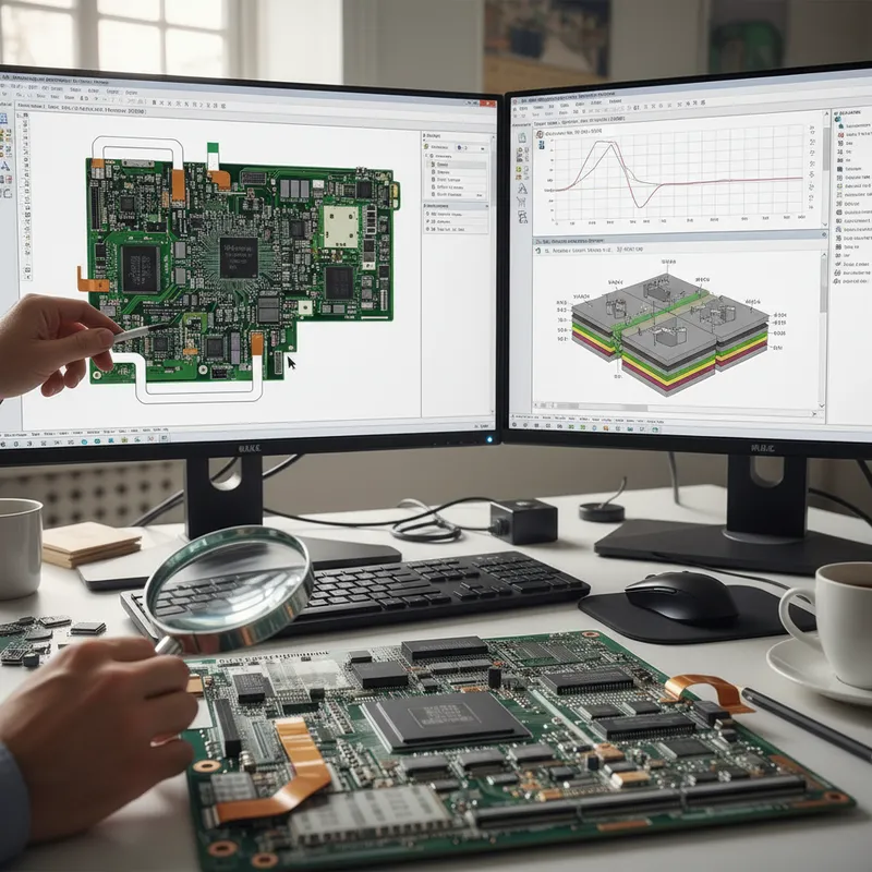
Printed Electronics is emerging to become as common as 3D printing. With this fast-emerging technology, new possibilities have come into the manufacturing arena, allowing engineers and designers to develop products in markets never before realized. New substrates and inks are being developed to address various applications, from biomedical to aerospace and consumer electronics.
With the emergence of many contract manufacturers possessing this capability, the cost is competitive. Quick-turn prototypes and volume production are now all possibilities, and with Altium 365® you stay connected directly with your manufacturer throughout the design process.
Join us for this informative webinar to see how Altium Designer natively addresses the design of Printed Electronics.
In This Webinar, We Will Explore The Following Areas:
- Routing techniques for today’s unique printed electronics designs
- How to connect with your manufacturer directly with Altium 365
- Create design packages ready for your manufacturer
- How to place vias for printed electronics
- Specifying your layer stack for printed electronics
Timing:
Thursday, 21st January 2021 | 02:30 PM to 03:30 PM
REGISTER NOW
Why printed electronics changes the PCB tooling conversation
Printed electronics is not just “PCB on flexible film.” The substrates (PET, PEN, paper, fabric, hybrid rigid-printed assemblies), the conductive inks (silver-based, carbon-based, copper-based, conductive polymers), the printing process tolerances (much wider than rigid PCB lithography), and the components (printed resistors and capacitors directly in the conductive pattern) each have to be modelled at the design tool level. Indian printed-electronics startups working in biomedical wearables, RFID/NFC tags, smart packaging, and IoT skin-mounted sensors hit each of these constraints in their first prototype run.
How Siemens Xpedition handles printed and hybrid electronics
GSAS Micro Systems is an authorized engineering partner in India. Xpedition Standard and Xpedition Enterprise approach printed electronics as a stack-up and design-rules problem, non-traditional substrates and conductive inks become material entries in the stack-up library, the routing rules adapt to ink-specific minimum trace widths and via constraints, and the manufacturing data flows through Valor NPI DFM sign-off against the printing-process equivalent of fabricator capabilities.
For hybrid rigid-printed assemblies, where a traditional rigid PCB carries the silicon and a printed-electronics flex extension carries sensors or antennas, Xpedition Enterprise’s rigid-flex + advanced packaging flow handles the boundary conditions consistently. The same design database covers the rigid section, the printed section, and the assembly.
For deeper coverage of how the two flows compare on stack-up management, layer rules, and manufacturing sign-off, see our Altium Designer vs Siemens Xpedition Standard for Indian PCB teams comparison.
Also appears in:
Need embedded development tools?
Talk to our application engineers for personalized tool recommendations.