
 SEGGER
 J-Link OB
Debug & TraceOn-board J-Link debug probe for OEM integration, a single-chip solution soldered directly onto evaluation and production boards. Available in India from GSAS.
Form Factor
Single-chip, on-board
Interface
JTAG, SWD, SWO
Architecture
Arm Cortex-M/A/R, RISC-V
VCOM
Built-in virtual COM port
Licensing
OEM evaluation & production
Overview
About J-Link OB
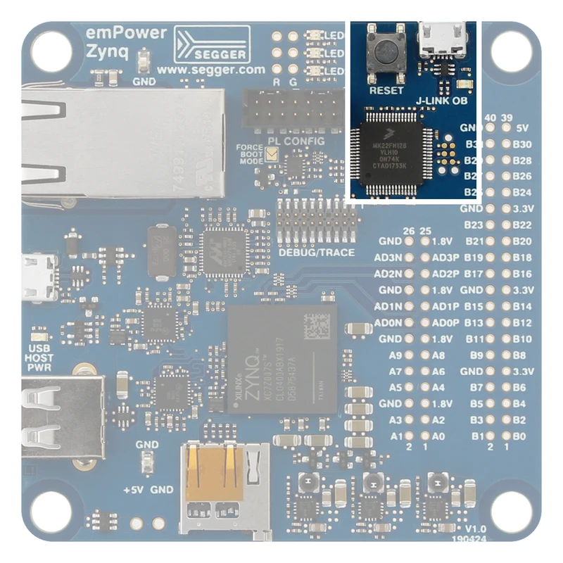
The J-Link OB (On-Board) is a microcontroller-based, single-chip J-Link implementation designed to be soldered directly onto evaluation boards and production hardware. Instead of requiring an external debug probe, the J-Link OB integrates JTAG, SWD, and SWO debug connectivity into the target board itself, providing out-of-the-box debug access through a standard USB connection with no additional hardware required by the end user.
OEM Integration and Licensing
SEGGER offers J-Link OB under multiple licensing models to match different use cases. Evaluation board manufacturers license J-Link OB to ship debug capability built into their development kits, giving customers immediate access to J-Link tools without purchasing a separate probe. For production use, dedicated licensing tiers cover fixed single-target internal use (FSTI), fixed single-target shipping products (FSTP), and detachable multi-target configurations for internal use and production (MTDI and MTDP), with a buy-out license available on request. GSAS provides licensing guidance and volume pricing for Indian OEMs integrating J-Link OB into their hardware platforms.
The J-Link OB supports tens of thousands of devices across Arm Cortex-M, Cortex-A, Cortex-R, and RISC-V families, and includes virtual COM port (VCOM) functionality for serial communication alongside debug where the OB implementation supports it (VCOM ships disabled and is enabled via the J-Link Configurator). A standard J-Link OB comes with the same software options as the J-Link BASE; the OB PLUS option adds Unlimited Flash Breakpoints, the Ozone debugger, and J-Flash for the board’s end users. Optional features include drag-and-drop programming and WebUSB programming support, making the J-Link OB a versatile on-board debug and programming solution.
Features
| Feature | Specification |
|---|---|
| Form Factor | Single-chip, soldered on-board |
| Debug Interface | JTAG, SWD, SWO |
| Architectures | Arm Cortex-M/A/R, RISC-V |
| Device Support | Tens of thousands of devices |
| Virtual COM Port | Built-in VCOM for serial communication |
| Drag & Drop | Optional drag-and-drop programming |
| WebUSB | Optional WebUSB programming support |
| Host Connection | USB (on-board USB interface) |
| External Crystal | Not required (K22 and STM32F072 implementations) |
| Software Options | Matches J-Link BASE; Unlimited Flash Breakpoints, Ozone, and J-Flash require the OB PLUS option |
| IDE Compatibility | Embedded Studio, Keil MDK, IAR, Eclipse, VS Code |
| Licensing | Evaluation board, FSTI, FSTP, multi-target detachable |
Watch the SEGGER J-Link OB introduction
The J-Link OB brings the full J-Link ecosystem to on-board implementations, ensuring that evaluation board users and OEM customers benefit from the same IDE compatibility, flash algorithm support, and software tools available with standalone J-Link probes.
J-Link OB Licensing in India from GSAS
J-Link OB is licensed rather than bought off the shelf, so the right first step is a conversation about your board volumes and use case. GSAS Micro Systems, an authorized engineering partner in India, guides Indian OEMs through evaluation-board and production licensing tiers with competitive pricing and short lead times, and supports the integration engineering from our offices in Bengaluru, Hyderabad, Chennai, Pune, Mumbai, and Delhi NCR. For standalone probes for your own lab, see the J-Link BASE or J-Link PRO. Contact GSAS to scope an OB licensing discussion.
Blog
SEGGER Insights

Meet the GSAS Team at electronica India 2026, Stall H3.I45
electronica India 2026 opens on 16 September at BIEC Bengaluru. The GSAS team is on the floor all three days at Stall H3.I45, and this is who you will be talking to and what they can show you.
J-Link Is Now Validated by ST for StellarStudio
STMicroelectronics has fully validated SEGGER J-Link for StellarStudio, the IDE for its Stellar automotive MCU family, and put the probe into continuous validation at Le Mans. What that changes for the toolchain review on a Stellar programme, from GSAS, an authorized engineering partner for SEGGER in India.
An AI Agent That Drives the Debugger: SEGGER and Embedder Connect J-Link to the Loop
SEGGER has given an AI coding agent direct control of J-Link and J-Trace: flash, breakpoints, memory inspection and live RTT on real silicon. The loop only works if the probe can read target RAM while the core runs, and GSAS field engineers know exactly where that breaks first.
Related products
More from SEGGER
All SEGGER products →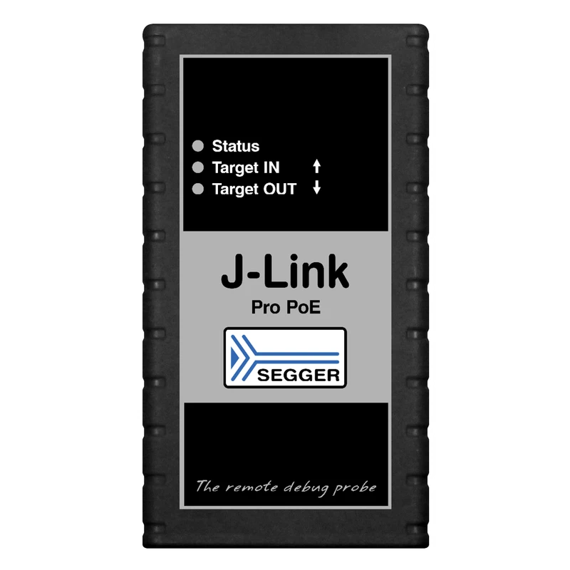
J-Link PRO PoE
Professional JTAG/SWD debug probe with USB, Ethernet, and Power over Ethernet, deploy in labs with a single cable. Available in India from GSAS.
View J-Link PRO PoE →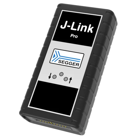
J-Link PRO
Professional JTAG/SWD debug probe with USB and Ethernet connectivity, supporting Arm Cortex-M/A/R and RISC-V architectures. India pricing and local support from GSAS.
View J-Link PRO →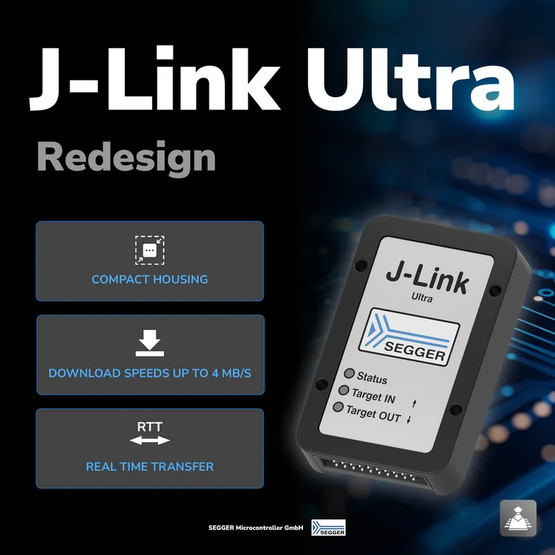
J-Link ULTRA
SEGGER's ultra-fast J-Link debug probe, now redesigned: compact USB-C housing, 4 MB/s download over USB 2.0 Hi-Speed, standard 20-pin JTAG/SWD connector. Buy J-Link ULTRA in India from GSAS Micro Systems.
View J-Link ULTRA →FAQ
Common questions about J-Link OB
What is the SEGGER J-Link OB?
How is the J-Link OB licensed in India?
Do end users need extra hardware to debug with a J-Link OB board?
Does the J-Link OB provide a serial port as well as debug?
Interested in J-Link OB?
Get pricing, an evaluation unit, or a technical consultation from our application engineers.