Thermal stress is one of the dominant wear-out mechanisms in deployed electronics, and the failure modes are well understood: solder joint fatigue from thermal cycling, electromigration acceleration at elevated temperatures, capacitor dielectric breakdown, and semiconductor junction degradation. Most follow Arrhenius-type behaviour, where the common engineering rule of thumb is that reaction-driven failure rates roughly double for every 10 degree Celsius rise in operating temperature.
Despite this, thermal management remains one of the most consistently under-addressed aspects of PCB design. The traditional approach, design the board, build a prototype, discover thermal problems during environmental testing, and then retrofit thermal solutions, is expensive, schedule-consuming, and almost always results in compromised solutions. A heatsink added after layout is never as effective as thermal-aware placement designed from the start.
The shift-left approach to thermal management means bringing thermal analysis into the design process early enough to influence fundamental design decisions: component placement, stackup selection, copper allocation, and airflow strategy. CFD-based thermal simulation is what makes that practical.
The Traditional Approach and Its Costs
In the traditional PCB development workflow, thermal analysis occurs after the board is designed and often after the first prototype is built. The sequence typically follows this pattern.
The electrical engineer designs the board for electrical performance: signal integrity, power distribution, EMC compliance. Component placement is driven by signal flow, routing efficiency, and noise isolation. Stackup selection is driven by impedance targets and layer count minimisation. Copper allocation is driven by current capacity and power plane requirements.
The mechanical engineer designs the enclosure based on the board outline, connector positions, and mounting requirements. Thermal management is addressed through general-purpose ventilation, slots in the enclosure, a fan if the power dissipation is high enough, based on experience and rule-of-thumb calculations.
The prototype is built and tested. Environmental testing reveals that one or more components exceed their rated junction temperature under worst-case operating conditions. The thermal problem may be localised (a single power stage running hot) or systemic (the overall enclosure temperature exceeding expectations).
The remediation options are all expensive. Adding a heatsink to an existing component requires mechanical clearance that may not exist. Adding forced-air cooling requires enclosure modifications, fan procurement, and acoustic analysis. Re-routing copper for thermal relief requires a board respin. Relocating a hot component away from a thermally sensitive component requires re-layout and re-verification.
Each of these remediation options costs weeks of schedule and significant engineering time. And each one is a compromise, a solution that fits within the constraints of the existing design rather than a solution that was designed into the product from the beginning.
What CFD Thermal Simulation Provides
Computational fluid dynamics solves the coupled airflow and heat transfer problem across the board and its surroundings. For electronics work the capability that matters is conjugate heat transfer: solving conduction through solids and convection in the surrounding fluid together, in one model, rather than treating them as separate problems joined by an assumed heat transfer coefficient.
The practical barrier has historically been meshing. General-purpose CFD tools require geometry simplification and meshing expertise that most electronics engineers do not have and should not need. Solvers aimed at electronics cooling address this with automatic mesh generation, which is what moves thermal analysis out of the specialist queue and into the design loop.
Cradle CFD from Cadence is the suite GSAS supports for this work. It provides two solvers: scSTREAM, a structured Cartesian solver optimised for electronics cooling, and scFLOW, a polyhedral unstructured solver for complex geometries such as automotive underhood and rotating machinery. Both include automatic meshing, conjugate heat transfer, radiation modelling, transient analysis, and built-in parametric study.
Component-Level Analysis
At the component level, thermal analysis calculates junction temperature based on the component’s thermal model, power dissipation, mounting configuration, and local thermal environment. A complete analysis accounts for all three heat transfer mechanisms: conduction through the PCB and component leads, convection from exposed surfaces to the surrounding air, and radiation exchange between surfaces.
For power semiconductors, this is particularly critical. A MOSFET or IGBT junction temperature that sits above the rated maximum does not just reduce lifetime, it can cause immediate parametric failure or thermal runaway. Junction temperature prediction is what allows the designer to verify thermal compliance before committing to hardware.
Board-Level Analysis
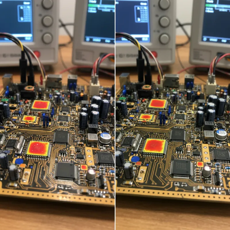
At the board level, the PCB is modelled as a composite structure: copper layers, dielectric layers, thermal vias, and surface finishes. The solver calculates the temperature distribution across the board, identifying hot spots where component power dissipation, inadequate copper spreading, or poor thermal via placement creates localised temperature elevation.
Board-level analysis is where thermal-aware placement delivers its greatest value. By evaluating the thermal impact of placement decisions during layout, the designer can position high-power components where the board’s thermal spreading capability is greatest, maintain adequate spacing between thermally sensitive components and heat sources, and allocate copper pour area for thermal relief where it will be most effective.
System-Level Analysis
At the system level, the model covers the complete product: PCB assembly, enclosure, ventilation features, and external environment. The analysis predicts airflow patterns through the enclosure, temperature distribution within the enclosed volume, and the thermal interaction between multiple boards in a multi-board system.
System-level analysis is essential for products where the thermal environment is defined by the enclosure and installation context rather than by the board alone. A PCB that is thermally compliant on an open bench may overheat when installed in a sealed enclosure or when adjacent to another heat-generating assembly.
Component Thermal Models
Accurate thermal simulation requires accurate thermal models of the components on the board. This is the input that most often limits result quality. Datasheet thermal resistance values (theta-JA, theta-JC) are measured under specific standardised conditions that rarely match the actual application, so using them directly as if they were application-independent constants is a common source of error.
The more defensible approach is a compact thermal model that represents the component’s internal structure, die, die attach, leadframe or substrate, mould compound, and exposed pad, and that holds up across a range of boundary conditions rather than at a single test condition. Two-resistor and DELPHI-style compact models exist for exactly this reason, and many component vendors publish them. Where a vendor model is not available, the practical fallback is to bound the problem: run the analysis at the optimistic and pessimistic ends of the plausible thermal resistance range and check whether the design decision changes.
Thermal Analysis Inside the Design Loop
The shift-left approach requires thermal analysis to be accessible during the design process, not only as a post-design verification step. In practice that means building the thermal model from the current state of the design, component placement, copper allocation, via placement, and stackup, and rebuilding it as those change, rather than modelling once at the end. How much of that transfers automatically depends on the tools in use; the discipline that matters is re-running the analysis while the layout is still movable.
This iterative workflow, place, analyse, adjust, re-analyse, converges on a layout that satisfies both electrical and thermal requirements. The key insight is that thermal analysis during layout is not an additional burden. It replaces the far more expensive cycle of prototype, test, redesign that occurs when thermal problems are found late.
The same argument applies at the mechanical boundary. For sealed enclosures where natural convection and radiation are the only heat dissipation mechanisms, the enclosure itself is a thermal component: its material, surface finish, and geometry directly affect internal temperature. Bringing the enclosure into the thermal model lets the mechanical engineer optimise it for thermal performance alongside structural and manufacturing requirements, instead of discovering the interaction after both designs are frozen.
What-If Analysis: Evaluating Thermal Solutions
Once a thermal problem is identified, the designer needs to evaluate potential solutions quickly and quantitatively. This is where parametric study and design-of-experiments capability earns its place, because the question is rarely “does this work” and usually “which of these five options works best”.
Heatsink selection. Evaluate different heatsink geometries, fin count, fin height, base thickness, and material, and predict their impact on junction temperature. A useful analysis accounts for the mounting interface (thermal pad, thermal tape, mechanical clip), the available airflow, and the interaction with adjacent components.
Airflow optimisation. For forced-air-cooled systems, evaluate fan placement, duct geometry, and inlet and outlet configuration. Predicted airflow velocity across each component lets the designer verify that adequate cooling reaches the highest-power parts and that dead zones of stagnant air are eliminated.
Thermal interface material selection. The interface between a component and its heatsink is often the dominant thermal resistance in the heat path. Comparing thermal pads, thermal paste, and phase-change materials quantifies the junction temperature impact, which matters because the best-performing TIM is not always the one that survives contact with manufacturing requirements for dispensing, placement, and rework.
Thermal via optimisation. For components with exposed thermal pads such as QFN and DFN packages, thermal vias provide a conduction path from the component to inner copper planes or the opposite side of the board. Via count, diameter, pitch, and fill (plated against filled) can each be swept to find the pattern that delivers the needed conduction without creating assembly problems.
Indian Applications
India’s electronics manufacturing landscape presents specific thermal management challenges that make shift-left thermal analysis particularly valuable.
Power electronics for electric vehicles. India’s EV transition is driving demand for motor controllers, battery management systems, onboard chargers, and DC-DC converters. These operate at high power densities in underhood environments where ambient temperatures are high. Thermal design is not a secondary concern in these applications, it is the primary design constraint, and verifying compliance at the design stage avoids committing to expensive prototype hardware.
Telecom outdoor equipment. India’s telecom infrastructure includes a large installed base of outdoor equipment, base station radios, small cells, and network switches, operating in sealed or semi-sealed enclosures under high summer ambients. Thermal management in these products relies primarily on conduction and natural convection, with forced air cooling reserved for high-power units. System-level analysis predicts internal temperatures under worst-case ambient conditions across India’s temperature range.
LED lighting. India’s LED lighting market is among the largest in the world, and LED driver boards operate in enclosed luminaire housings with limited cooling options. LED performance and lifetime are directly related to junction temperature, which makes thermal management a quality factor rather than a nice-to-have, and it means the driver board layout and the luminaire thermal design have to be optimised together.
Industrial drives. Variable frequency drives, servo controllers, and industrial power supplies dissipate significant power in enclosed control cabinets. The thermal interaction between multiple drives in one cabinet is a systemic problem that cannot be addressed by analysing individual units in isolation, which is exactly the case for modelling the cabinet-level environment including each unit’s contribution to the shared load.
The Shift-Left Imperative
The economic argument for shift-left thermal analysis is straightforward. A thermal problem found during design costs minutes to analyse and hours to fix. A thermal problem found during prototyping costs weeks to diagnose and weeks to remediate. A thermal problem found during field deployment costs the product’s reputation and the company’s customer relationships.
What makes shift-left practical is tooling that electronics engineers can drive themselves, that meshes without a specialist, and that returns results fast enough to support iterative exploration rather than a single end-of-project check.
For Indian electronics companies designing products that must operate in demanding thermal environments, and in India nearly every environment is thermally demanding, shift-left thermal analysis is not a luxury. It is a competitive necessity.
Ready to implement thermal-aware design? Contact GSAS Micro Systems for Cradle CFD evaluation, thermal analysis workflow setup, and training on shift-left thermal management methodologies. Our engineers work with design teams across Bengaluru, Hyderabad, Chennai, Pune, Mumbai, and Delhi NCR to establish thermal analysis processes that catch problems during design, not during field deployment. Contact GSAS to discuss your requirements.
Also appears in:
Interested in Cadence tools?
Talk to our application engineers for personalized tool recommendations.
More from Cadence
View all →
MSC Software Is Now Part of Cadence: What the Hexagon Acquisition Means for Indian Simulation Teams
28 May · 6 min

Adams Multibody Dynamics: The Standard for Vehicle Dynamics Simulation in India
5 Apr · 6 min

MSC Nastran: Six Decades of Structural FEA and Why It Still Matters in India
4 Apr · 6 min
Actran Acoustic Simulation: Solving the EV NVH Challenge in India
3 Apr · 6 min

Emulating Processor Power for Thermal Testing: Why Constant Power
7 Oct · 7 min

CRPS and Rack Power Supply Testing: The Six Tests That Matter
7 Oct · 7 min