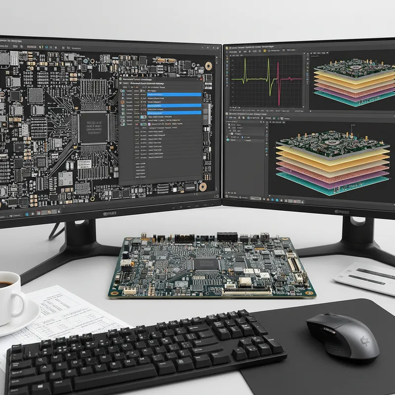
The definition of the PCB layer stack is a critical element of successful printed circuit board design. No longer just a series of simple copper connections that transfer electrical energy, the routing of many modern PCBs is designed as a series of circuit elements, or transmission lines.
Please join our webinar to discuss how Altium Designer’s advanced layer stack manager supports all aspects of layer stack configuration.
Agenda
- Layer Stackup Improvements
- Material Library
- Micro Via and back drill support
- Impedance Profile management
- Printed Electronics support (conductive ink)
- Live Demo
- Q&A
Timing:
Friday, 9th July 2021 | 02:30 PM to 03:30 PM
Webinar Recording
Why stack-up management decides high-speed performance
Layer stack-up is the foundation everything else in a high-speed PCB design rests on. Once the stack is committed, the controlled-impedance trace widths, differential pair geometries, decoupling strategy, and EMC margin are all locked in, and changing the stack mid-design typically means redoing routing on every signal layer. Indian PCB teams designing for DDR4/5, PCIe Gen5/6, USB4, 5G FR1/FR2, and 100G+ Ethernet are increasingly stack-up-driven from the first day of the project.
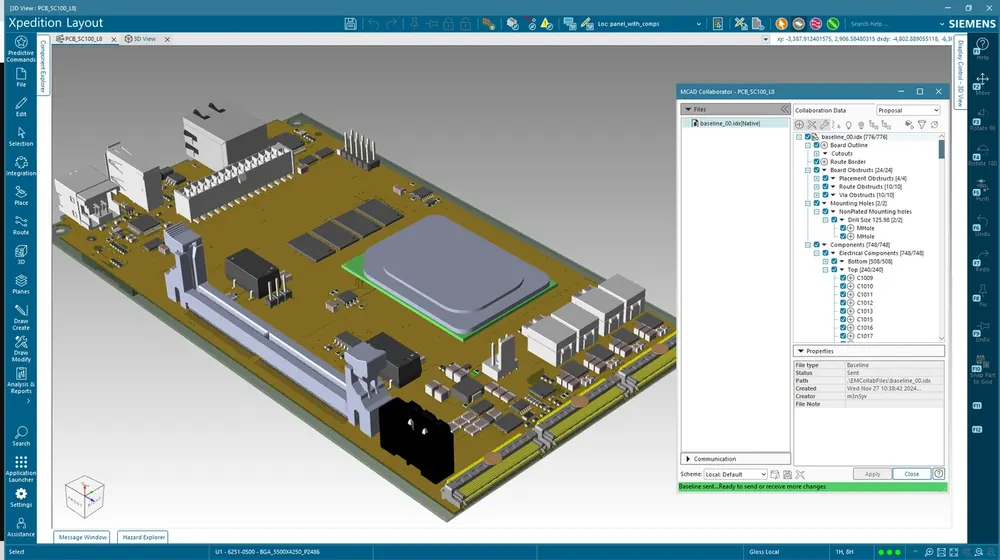
How Siemens Xpedition’s stackup flow goes deeper
GSAS Micro Systems is an authorized engineering partner in India. The Xpedition stack-up workflow integrates tightly with the HyperLynx Z Planner, single-ended and differential impedance is calculated against actual material library data from your fabricator, micro-via and back-drill structures are first-class objects in the stack-up rather than annotations, and the impedance profiles flow into the routing rules without manual sync between tools.
For Indian teams designing for high-speed serial lanes, the practical advantage shows up in two places:
- Pre-layout topology exploration: sweep stack-up choices against impedance, insertion loss, and crosstalk targets before committing to materials. HyperLynx Z Planner does this on the Xpedition Standard seat (with token-based SI add-on) or Xpedition Enterprise flagship.
- Post-layout sign-off: once routed, the actual impedance is extracted from the design and verified against the spec. No manual re-entry of stack-up data into a separate SI tool.
For Indian teams comparing the stack-up workflow head-to-head, see our Altium Designer vs Siemens Xpedition Standard for Indian PCB teams guide.
About GSAS Webinar Series
GSAS Micro Systems regularly hosts webinars, workshops, and technical seminars to help India’s embedded engineering community stay current with the latest tools, techniques, and industry standards. Our events feature hands-on demonstrations and expert guidance from our applications engineering team.
Request a private session for your engineering team, or browse our complete event archive.
Also appears in:
Need embedded development tools?
Talk to our application engineers for personalized tool recommendations.