
If you run a PCB fabrication line, an EMS NPI desk, or a DFM cell that signs off layouts before they go to the fab, the Valor NPI 2604 release is the one to read carefully. It is not a UI refresh. It is a set of targeted DFM rules and data-flow upgrades that close the gap between what the designer drew and what your process can actually build.
Five themes carry the release: IPC-4761 via-type awareness flowing through the pad stack into manufacturing analysis, three sliver and acid-trap checks migrated into the Analysis Definition Manager (ADM), perimeter-based copper coverage analysis for SMD and BGA pads, new through-hole lead-length constraints driven by the Valor Parts Library, and tighter Cadence Allegro interoperability for advanced degassing shape rotation.
This recap walks each one in the order the Siemens EDA team published it, with the full demo videos embedded and the engineering detail filled in from what the presenters actually show on screen.
Smarter DFM with IPC-4761 via-type awareness
For years the via story in a manufacturing flow has had a hole in it. Designers would draw a via, then describe its finishing intent, tented, plugged, capped, filled, somewhere off to the side on a fab drawing. That drawing was a separate artefact, sometimes a separate PDF, and it never travelled cleanly with the design data. Pre-fab DFM had to guess.
Valor NPI 2604, paired with Xpedition 2604, closes this gap. Via type can now be declared per via inside Xpedition’s pad stack editor, using the seven via type classifications defined in IPC-4761. Each layout via is tied to a specific surface, and the via type selections are made available against that via directly. Layout geometry is not impacted, the assignment is metadata that travels with the design.
When ODB++ is generated, those via types are automatically extracted as a drill-type attribute. Valor NPI consumes the attribute and exposes it in design status reporting under a dedicated IPC-4761 via-type heading, listing the via types present, the surfaces they apply to and the count per type. The digital twin gets sharper, the fab drawing gets thinner, and signal integrity and manufacturing analysis can finally reason about the actual via stack the board will be built with.
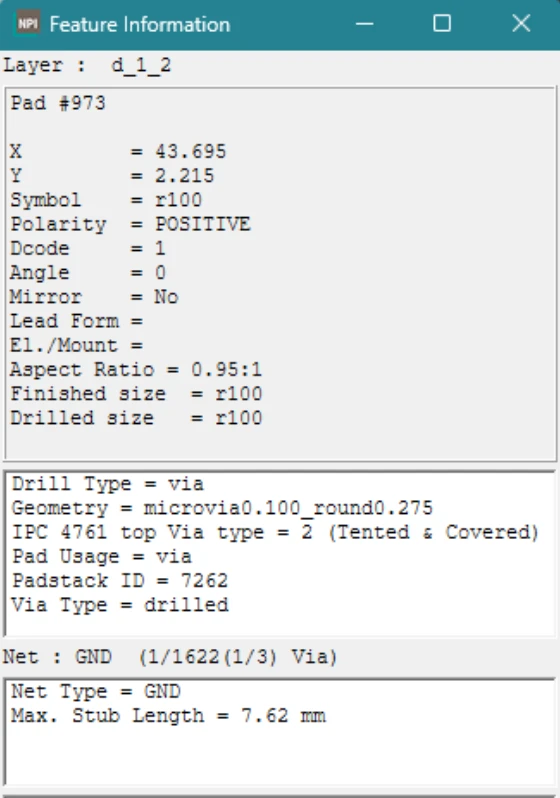 Figure 1: IPC-4761 via type values are reflected in the drill-type attribute on each via and flow into Valor NPI analysis constraints.
The seven IPC-4761 via types now selectable per via are:
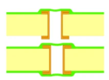 Tented
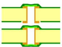 Tented and covered
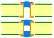 Plugged
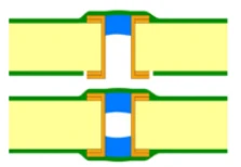 Plugged and covered
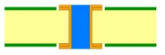 Filled
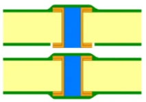 Filled and covered
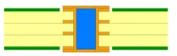 Filled and capped
Figure 2: The seven IPC-4761 via types selectable per via in Xpedition’s pad stack editor.
Once the via type is present as an attribute, Valor NPI 2604 turns it into something a DFM engineer can actually constrain on. The release ships four new constraints that key off the IPC-4761 attribute:
- Test Point to Uncapped Via Spacing: keeps the test pad away from a via that has not been capped, where flying-probe and ICT contact would otherwise risk a short or unreliable touchdown.
- Via Pad Capped on Both Sides of the Board: verifies symmetry where the manufacturing process demands it.
- Capped Via Under Component: catches the classic via-in-pad failure mode where an uncapped via sits beneath a BGA or QFN.
- IPC-4761 Covered Via Missing Solder Mask: flags vias whose declared coverage finish is inconsistent with what the solder-mask artwork actually delivers.
The Siemens EDA demo walks through how the attribute travels, pad stack editor to design status to ODB++ to Valor analysis, and the key engineering point lands cleanly: “Valor NPI is fully integrated and streamlines the design to manufacturing workflow, allowing enhanced capability for accurate analysis of signal integrity and manufacturing.”
For Indian fab houses dealing with mixed via stacks on the same panel, some vias intended for via-in-pad with conductive fill, some plain tented signal vias, some test-point vias that must stay uncapped, the move is straightforward to internalise. Stop reading the fab drawing as a free-text annotation. Read the IPC-4761 attribute on the ODB++ and constrain against it.
Sliver and acute-angle checks migrated into the Analysis Definition Manager
Three checks that long-time Valor users will recognise from the older DFS Actions menu in Graphics Station, photoresist sliver detection, copper surface sliver and acid trap detection, have been migrated into the Analysis Definition Manager. This is not a cosmetic move. ADM is where the configurable, repeatable, project-templated analyses live, and putting these three checks into it means they can finally be versioned, shared and run consistently across teams.
 Figure 3: Copper surface sliver, acid trap detection and photoresist sliver detection are the three checks brought into the Analysis Definition Manager in Valor NPI 2604.
The Siemens EDA presenter is explicit about provenance: “The request for these checks came through the Valor Community Ideas site and was voted on by Valor customers.” That is the customer-driven roadmap working as intended. If you have a check you want surfaced, the Ideas site is the path.
What each check actually does, in the engineering sense:
- Photoresist sliver detection: searches for thin areas of photoresist between adjacent copper edges. These thin strips are where etchant accumulates during fabrication, and the result is over-etching that narrows or breaks the adjacent copper feature. The constraint reports on both positive and negative copper layers.
- Copper surface sliver (shown in the results window as splinter), flags locations where copper extends outward from a feature as a narrow wedge or finger. The risk is mechanical: the sliver may not adhere properly and can break free during fabrication, contaminating the panel and other boards on it. The constraint applies on both positive and negative layers.
- Acid trap detection (shown in the results window as acute angle), looks for acute angles formed in the photoresist between adjacent copper edges. The acute angle traps etchant, creating an acid trap during fabrication that locally over-etches the copper and degrades long-term reliability.
The 2604 release exposes two new configuration variables to control the geometry of what counts as a violation:
- One variable governs the maximum length of the base of the sliver that should be considered.
- The second variable sets the maximum angle between edges for the acid-trap analysis.
That tunability matters. Different fabricators have different process windows. A check that fires too aggressively against a fab with tight etchant control creates noise and ignored warnings; one that fires too loosely lets defects through. The two new variables let a DFM cell calibrate the checks to the real capability of the line they are validating against.
SMD and BGA pad-perimeter copper coverage
Valor NPI 2604 turns “is this pad well-connected to copper?” into a measurable, constrainable check. For every SMD and BGA pad, the tool now evaluates the percentage of the pad’s perimeter that is in direct contact with copper, and flags the pad when the value falls outside a defined window, too high or too low.
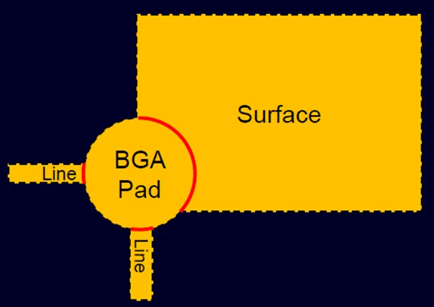 Figure 4: Valor NPI 2604 reports the percentage of a toeprint’s perimeter embedded in the connected copper.
The reason the band exists in both directions matters for an assembly engineer:
- Excessive copper connection turns the pad into a heat sink during reflow. The copper pulls heat away from the joint, causing uneven reflow, tombstoning on small passives and outright cold joints on larger packages. This is the classic root cause of an SMT line tuning the profile chasing a phantom oven problem.
- Insufficient copper connection leaves the pad mechanically weak, reduces conducted heat dissipation in operation and gives the joint less margin against vibration and thermal cycling.
The check is a quantitative replacement for the “looks fine to me” pad-thermal review. For Indian EMS lines running mixed product on the same reflow oven, automotive ECUs, consumer modules, telecom line cards, the rule means design issues that would have shown up as yield loss on the reflow side get caught at DFM.
Verifying through-hole lead length against board thickness
The Valor Parts Library (VPL) carries mechanical data about each component, including pin and lead length for through-hole and press-fit parts. Valor NPI 2604 adds new ADM constraints that use that data to verify whether the lead can actually be assembled into the board you have designed.
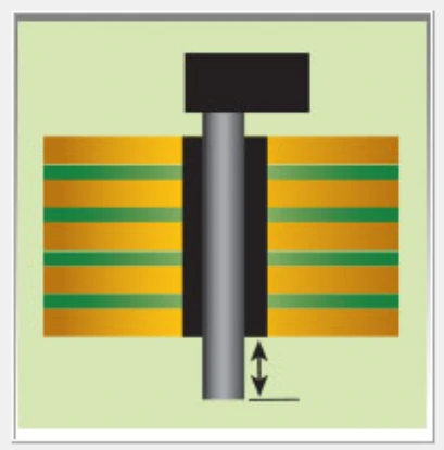 Figure 5: Excessive lead length relative to board thickness flagged by Valor NPI 2604.
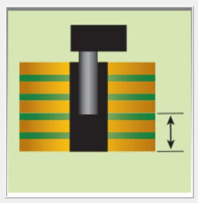 Figure 6: Insufficient lead length relative to board thickness flagged by Valor NPI 2604.
The constraints work in both directions:
- Excessive lead length: the lead protrudes too far past the secondary side after assembly. The risks are mechanical interference with adjacent assemblies, shorting to chassis or shields, and rework cost in lead trimming after wave or selective solder.
- Insufficient lead length: the lead does not reach far enough through the board to give a reliable solder joint. The result is poor wicking, weak fillet formation and low pull strength.
The check is particularly relevant for connector-heavy designs, backplane connectors, press-fit power pins, large-pitch power-stage through-hole devices, where the component datasheet and the board stack-up have to be reconciled before the panel ships. Reading the lead length out of VPL means the DFM engineer does not have to maintain a parallel spreadsheet of pin lengths per part number.
Cadence Allegro: exact degassing-shape rotation
Valor NPI 2510 introduced support for advanced degassing shapes; the 2604 release closes the last interoperability gap with Cadence Allegro. The exact rotation of degassing shapes is now imported from Allegro for versions SPB24.1 ISR007 and SPB25.1 ISR002. The rotation set in Allegro is preserved through to Valor, the degassing shapes are now rotated along the traces based on the rotation set in the Allegro design, not approximated.
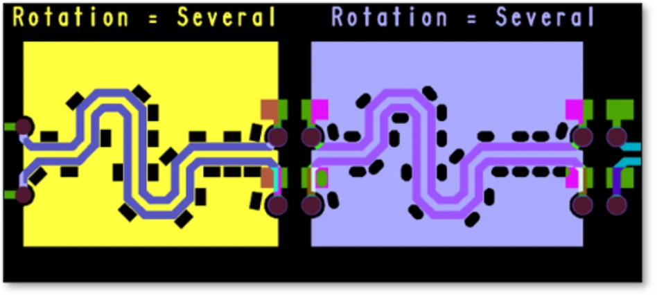 Figure 7: Degassing shapes are now rotated along the traces based on the rotation set in Allegro.
For Indian DFM houses that act as the bridge between Allegro-using design teams and Valor-driven manufacturing analysis, this removes a class of false positives that have nagged the workflow since degassing shapes started being used widely. The geometry that ships to the fab now matches the geometry the designer drew.
Why this matters for Indian engineering teams
The five changes in Valor NPI 2604 read like a checklist of the friction points an Indian PCB engineering team meets every quarter.
For EMS sites in Pune and contract manufacturers in Chennai that take in design data from multiple OEMs in a week, automotive ECU programs from European Tier-1s, telecom line cards from North American customers, industrial IoT boards from domestic startups, the IPC-4761 via-type attribute means no more chasing the fab drawing for a definitive statement of via finish. The intent is in the ODB++; the analysis runs against it; the report is unambiguous.
For DFM cells in Bengaluru that review layouts before release, the sliver and acid-trap checks moving into ADM means the analyses are now templated alongside the rest of the project’s DFM rules. A project that has signed off once can be re-validated against the same configured analysis, with the new sliver-length and angle thresholds tuned to the actual fab’s process window. The check is now versionable in the same way the rest of the constraint set is.
For NPI engineers supporting automotive ECU programs on the Hosur–Bengaluru corridor and defence PCB programs feeding into integration houses across Hyderabad and Visakhapatnam, the through-hole lead-length verification and the SMD/BGA pad-perimeter check catch two classes of yield-killer before the first panel runs. The lead-length rule kills the late-stage discovery that a connector pin does not reach through the assembled stack. The pad-perimeter rule kills the tombstoning that would have shown up only on the second SMT lot.
For design service houses in Delhi NCR and Mumbai that work in Cadence Allegro and hand off to Indian fabricators, the exact degassing-shape rotation fix means one less round-trip discrepancy to explain on a NPI call.
The connective tissue across the five features is the same: push DFM left, into the design environment, with data formats and constraint definitions that are precise enough to be acted on without back-and-forth.
FAQ
What Xpedition version do I need to flow IPC-4761 via types through to Valor NPI 2604? Xpedition 2604. The pad stack editor in 2604 is where the IPC-4761 via type is set per via, and the attribute is carried through ODB++ to Valor NPI 2604 for analysis. The two releases are designed as a paired flow.
Where do the photoresist sliver, copper surface sliver and acid trap detection checks live in 2604? Inside the Analysis Definition Manager (ADM). In earlier releases they sat under the DFS Actions menu inside Graphics Station. The migration means they are now part of the templated, project-level analysis configuration rather than an ad-hoc action.
How do I tune the sliver and acid-trap checks to my fabricator’s process? Two new configuration variables ship with the release. One sets the maximum length of the base of the sliver to be considered; the other sets the maximum angle between edges for acid-trap analysis. Calibrate them against your fabricator’s published process capability.
What appears in the results window for these checks? The copper surface sliver check reports as splinter. The acid trap detection check reports as acute angle. Photoresist sliver detection is reported by name. The naming is worth bookmarking when triaging results.
Which Allegro versions does Valor NPI 2604 support for the exact degassing-shape rotation import? Cadence Allegro SPB24.1 ISR007 and SPB25.1 ISR002. Designs from those versions carry the rotation attribute correctly into Valor.
Does the SMD and BGA pad-perimeter copper coverage check work for both excessive and insufficient connections? Yes. The check reports both ends of the spectrum against a defined threshold, so the same constraint catches the heat-sinking problem on a flooded pad and the mechanically weak joint on an under-connected pad.
Where GSAS comes in
GSAS Micro Systems is the Siemens EDA engineering partner for India. We support Indian PCB design, DFM and NPI teams on Xpedition, Valor NPI and HyperLynx, installation, configuration of ADM templates against the fab houses you actually use, integration with Cadence Allegro and PADS environments, and rollouts that move teams from one-off DFM at the end of the project to constraint-driven DFM running alongside the layout.
If you want to evaluate Valor NPI 2604 alongside Xpedition Standard, the Xpedition Standard free trial is the right starting point, it includes 12 cloud Valor DFM runs per year and gives a layout engineer a working view of the 2604 flow without procurement friction.
Start the Xpedition Standard 30-day trial · Talk to the GSAS Siemens EDA team · Contact us
Related reading
Also appears in:
Interested in Siemens EDA tools?
Talk to our application engineers for personalized tool recommendations.
More from Siemens EDA
View all →
India's EDA Moment: Why Design Tool Demand Is Growing, and the Engineering Careers It Creates
21 Sept · 9 min

AI and Complexity Are Redrawing EDA: Siemens on the Trillion-Transistor Era
13 Sept · 6 min

Calibre Vision AI: Bringing Order to DRC Debug at Advanced Nodes
24 Aug · 4 min

Siemens EDA EBS Expert Series: 6 Free PCB Design Webinars (Jul-Aug 2026)
20 Jul · 8 min

Emulating Processor Power for Thermal Testing: Why Constant Power
7 Oct · 7 min

CRPS and Rack Power Supply Testing: The Six Tests That Matter
7 Oct · 7 min