
 SEGGER
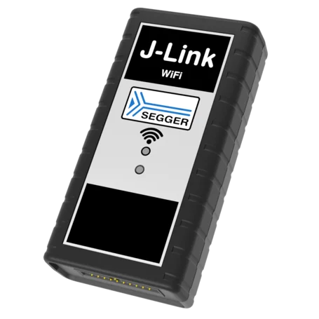
 J-Link WiFi
Debug & TraceWireless JTAG/SWD debug probe with WiFi and USB connectivity, USB powered so it can share the target's power source. Authorized India partner, GSAS Micro Systems.
Connectivity
WiFi 802.11 b/g/n (2.4 GHz) + USB 2.0
WiFi Speed
Up to 1 MB/s
Power
USB powered, max 220 mA @ 5 V
SWO
Up to 30 MHz
Cores
Cortex-M/A/R, RISC-V
Overview
About J-Link WiFi
The J-Link WiFi cuts the host data cable for embedded debugging, connecting to targets over WiFi 802.11 b/g/n (2.4 GHz). This removes the physical constraint that a USB cable to the host PC imposes on debug workflows, opening up use cases that are impossible or impractical with wired probes.
The probe is USB powered (max. 220 mA at 5 V), so it can share the same power source as the target device, a bench supply, the target’s own USB port, or a compact power bank, while the debug data travels over the wireless link. When WiFi is impractical or maximum speed is needed, the built-in USB 2.0 Hi-Speed port provides standard wired J-Link operation, making the WiFi variant a versatile choice that works in both wireless and wired scenarios.
All J-Link features are available wirelessly: unlimited flash breakpoints, RTT, SWO, and GDB Server with full IDE compatibility. Download speeds reach up to 1 MB/s over WiFi, sufficient for most firmware images and iterative debug cycles. A built-in web server handles TCP/IP configuration from any browser on the network, and initial setup takes two J-Link Commander commands over USB.
Wireless Debug Use Cases
- Environmental chambers: debug temperature/humidity tests without routing a data cable through the chamber wall, powering the probe from the fixture inside
- Sealed and hard-to-reach targets: debug boards mounted deep inside racks or machinery where a host USB cable cannot reach
- Moving platforms: debug robotics, conveyor systems, and rotating machinery powered from the platform’s own 5 V supply, with no data cable to snag
- Remote labs: share a single J-Link WiFi across multiple developers connecting from different workstations
- Distance from the bench: keep the host PC away from high-temperature or electrically noisy equipment during debug
- Production floors: debug units on the assembly line without routing host cables across work cells
Features
| Feature | Specification |
|---|---|
| WiFi Standard | 802.11 b/g/n (2.4 GHz) |
| WiFi Speed | Up to 1 MB/s download |
| Host Interface | WiFi + USB 2.0 Hi-Speed (fallback) |
| Power | USB powered, max. 220 mA @ 5 V |
| Debug Interface | JTAG, SWD (cJTAG supported) |
| Interface Speed | Max. 15 MHz, SWO up to 30 MHz |
| Target Voltage | 1.2 V to 5 V |
| Architectures | Arm Cortex-M/A/R, RISC-V |
| Flash Breakpoints | Unlimited |
| Web Interface | Built-in web server for TCP/IP configuration |
| Dimensions | 103 x 53 x 28 mm, 70 g |
| Support | 12 months SEGGER Basic Support included |
| IDE Compatibility | Embedded Studio, Keil MDK, IAR, Eclipse, VS Code |
Watch the SEGGER J-Link WiFi introduction
Setup is straightforward: connect the probe over USB once, set the network name and password with the SetWifi commands in J-Link Commander, and a solid green LED confirms the probe is on the network. From there, any J-Link-compatible software reaches it wirelessly, and J-Link Remote Server extends access beyond the local network.
Buy J-Link WiFi in India from GSAS
GSAS Micro Systems, an authorized engineering partner in India, supplies the J-Link WiFi with competitive pricing and short lead times, INR invoicing, and GST documentation. Our engineers in Bengaluru, Hyderabad, Chennai, Pune, Mumbai, and Delhi NCR help teams configure wireless debug on lab and factory networks and choose between the WiFi, J-Link PRO, and J-Link ULTRA models for their workflow. Request a quote or order from the GSAS store.
Blog
SEGGER Insights

Meet the GSAS Team at electronica India 2026, Stall H3.I45
electronica India 2026 opens on 16 September at BIEC Bengaluru. The GSAS team is on the floor all three days at Stall H3.I45, and this is who you will be talking to and what they can show you.
J-Link Is Now Validated by ST for StellarStudio
STMicroelectronics has fully validated SEGGER J-Link for StellarStudio, the IDE for its Stellar automotive MCU family, and put the probe into continuous validation at Le Mans. What that changes for the toolchain review on a Stellar programme, from GSAS, an authorized engineering partner for SEGGER in India.
An AI Agent That Drives the Debugger: SEGGER and Embedder Connect J-Link to the Loop
SEGGER has given an AI coding agent direct control of J-Link and J-Trace: flash, breakpoints, memory inspection and live RTT on real silicon. The loop only works if the probe can read target RAM while the core runs, and GSAS field engineers know exactly where that breaks first.
Related products
More from SEGGER
All SEGGER products →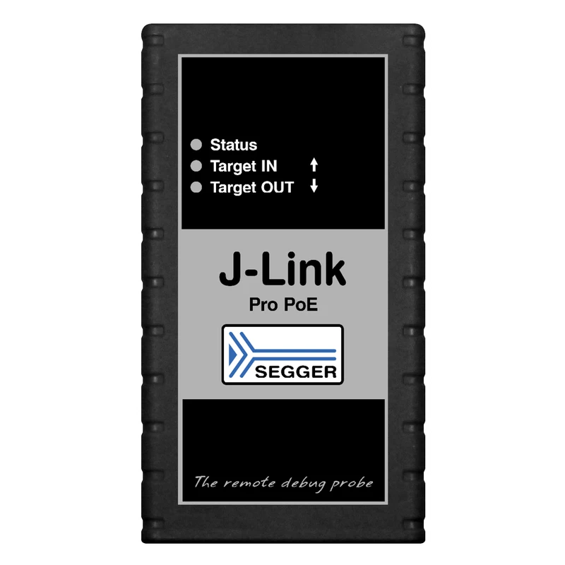
J-Link PRO PoE
Professional JTAG/SWD debug probe with USB, Ethernet, and Power over Ethernet, deploy in labs with a single cable. Available in India from GSAS.
View J-Link PRO PoE →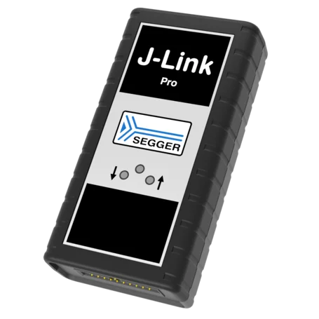
J-Link PRO
Professional JTAG/SWD debug probe with USB and Ethernet connectivity, supporting Arm Cortex-M/A/R and RISC-V architectures. India pricing and local support from GSAS.
View J-Link PRO →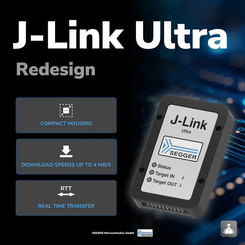
J-Link ULTRA
SEGGER's ultra-fast J-Link debug probe, now redesigned: compact USB-C housing, 4 MB/s download over USB 2.0 Hi-Speed, standard 20-pin JTAG/SWD connector. Buy J-Link ULTRA in India from GSAS Micro Systems.
View J-Link ULTRA →FAQ
Common questions about J-Link WiFi
What is the price of the SEGGER J-Link WiFi in India?
How do I set up the J-Link WiFi on my network?
Does the J-Link WiFi have a battery?
When does a wireless debug probe make sense over USB?
Can the J-Link WiFi also be used as a normal USB probe?
Interested in J-Link WiFi?
Get pricing, an evaluation unit, or a technical consultation from our application engineers.