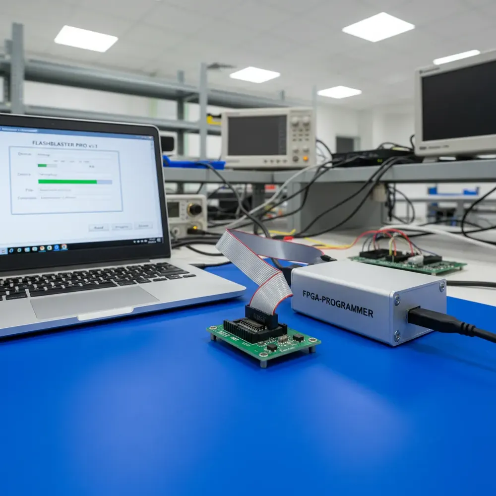
Quad SPI (QSPI) flash programming uses four data lines instead of the standard single MOSI/MISO pair, enabling 4x the data throughput for the same clock frequency. The Promira Serial Platform supports Quad SPI and Dual SPI modes at clock speeds up to 80 MHz, making it the fastest host adapter in the Total Phase lineup for flash programming applications. Combined with Flash Center Software’s GUI-based programming interface, the Promira delivers production-grade QSPI flash programming without writing a single line of code.
Hardware Setup
For this example, we use a Micron N25Q032A, a 32 Mbit (4 MB) QSPI flash that operates at 1.8V. The Promira’s integrated level shifting handles the voltage translation from the host PC’s USB interface to the 1.8V I/O required by the flash device.
Connection
Connect the Promira to the flash target via a 10-pin or 34-pin ribbon cable. For QSPI operation, the Promira uses four data lines:
| Promira Pin | Signal | Flash Pin |
|---|---|---|
| SCLK | SPI Clock | CLK |
| MOSI/IO0 | Data 0 | DQ0 |
| MISO/IO1 | Data 1 | DQ1 |
| IO2 | Data 2 | DQ2 |
| IO3 | Data 3 | DQ3 |
| SS | Chip Select | CS# |
| GND | Ground | VSS |
Promira Configuration
1. Host interface: Connect via USB (bench use) or Ethernet (production floor).
2. I/O voltage: Set the supplementary I/O power to 1.8V in the Promira configuration utility, this sets the level shifter output voltage.
3. Target power: Enable target power if the flash device is not otherwise powered.
4. SPI mode: Set to Quad I/O in Flash Center.
Flash Center Programming Workflow
1. Select Target Device
In Flash Center, navigate to Operations > Select Target. The built-in device database includes the N25Q032A and thousands of other SPI and QSPI flash devices. Flash Center automatically configures the correct command set, page size, sector size, and timing parameters for the selected device.
2. Choose Operation
Flash Center supports several programming modes:
| Mode | Description |
|---|---|
| Program + Verify | Write data and read back to confirm (recommended) |
| Program (with erase) | Erase sectors before programming |
| Program (no erase) | Write without prior erase (for pre-erased devices) |
| Read | Read flash contents to file |
| Verify | Compare flash contents against a reference file |
| Erase | Sector or chip erase |
3. Execute
Select your firmware binary file and click Execute. Flash Center handles the complete programming sequence automatically:
1. Erase: issues Sector Erase (0xD8) commands for each 64 KB sector that will be written.
2. Program: uses Quad Input Fast Program (0x32) to write data in 256-byte pages across all four data lines simultaneously.
3. Verify: uses Quad Output Fast Read (0x6B) to read back the programmed data and compare byte-by-byte against the source file.
Key N25Q032A Parameters
| Parameter | Value |
|---|---|
| Capacity | 32 Mbit (4 MB) |
| Sectors | 64 (64 KB each) |
| Subsectors | 1,024 (4 KB each) |
| Page Size | 256 bytes |
| Write Enable | 0x06 (required before every program/erase) |
| Quad Input Fast Program | 0x32 |
| Quad Output Fast Read | 0x6B |
Why Promira for QSPI
The Promira’s 80 MHz SPI clock with Quad I/O delivers a theoretical data throughput of 40 MB/s (80 MHz x 4 bits / 8 bits per byte). In practice, throughput is limited by the flash device’s page program time and the overhead of erase operations, but the Promira’s pipelined queue architecture minimizes host-side latency between pages.
For teams that have been using the Aardvark (8 MHz, standard SPI only) or Cheetah (40+ MHz, standard SPI only), the Promira’s Quad SPI capability represents a significant productivity improvement for flash programming workflows, particularly for devices with large firmware images (multi-megabyte) that benefit from the 4x data lane parallelism.
GSAS Micro Systems provides the Promira Serial Platform with guidance on SPI Active application licensing (Level 1/2/3), flash target device selection, and production programming fixture integration for manufacturing teams across India.
Also appears in:
Interested in Total Phase tools?
Talk to our application engineers for personalized tool recommendations.
More from Total Phase
View all →
Aardvark vs Cheetah vs Promira: Total Phase Host Adapter Guide (India)
17 Jul · 6 min
Automated EV Charger Test Bench in India: GW Instek AC Source, DC Load and Battery Emulator
6 Jun · 16 min
Best Logic Analyzer in India (2026): A Vendor-Neutral Buying Guide for Embedded Teams
5 Jun · 10 min
Capturing I²C/SPI Data to Train Edge AI: A Protocol-Analyzer Workflow for Indian Embedded Teams
4 Jun · 9 min

Emulating Processor Power for Thermal Testing: Why Constant Power
7 Oct · 7 min

CRPS and Rack Power Supply Testing: The Six Tests That Matter
7 Oct · 7 min