Digital signal processing on microcontrollers is limited by sequential execution, the processor handles one operation at a time, and the achievable sample rate depends on how fast the processor can execute the filter algorithm. FPGAs remove this bottleneck. Every multiply-accumulate operation in a FIR filter, every butterfly computation in an FFT, every comparison in a threshold detector can execute in parallel, in dedicated hardware, at the FPGA clock rate.
The result is signal processing throughput that scales with the available hardware resources rather than with processor clock speed.
For Indian engineers in Bengaluru, Pune, Chennai, and Hyderabad working on audio processing, sensor signal conditioning, communications, and instrumentation, FPGA-based DSP provides capabilities that microcontrollers and DSP processors cannot match in throughput and deterministic timing.
The Hardware Setup
A practical FPGA DSP development setup using Digilent components:
FPGA board: Digilent Arty A7 (35T or 100T). The Artix-7 FPGA provides DSP slices, dedicated hardware multiply-accumulate blocks, that implement DSP operations efficiently. The 35T has 90 DSP slices; the 100T has 240. Each DSP slice implements a 25x18-bit multiply followed by a 48-bit accumulate, running at the FPGA clock rate.
ADC input: Digilent PmodAD1 (12-bit, 1 MSPS, 2-channel) or PmodAD2 (12-bit, 1 MSPS, 4-channel) for signal acquisition. The Pmod interface connects directly to the Arty A7’s Pmod connectors, no additional wiring or interfacing needed.
DAC output: Digilent PmodDA2 (12-bit, 2-channel) for signal output. Completes the signal chain for real-time processing applications where the processed signal must be output as an analog waveform.
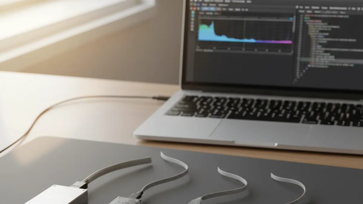
Alternative: Analog Discovery 3. For development and testing, the Analog Discovery 3 serves as both the signal source (waveform generator) and the measurement instrument (oscilloscope), generating test signals into the FPGA’s ADC input and capturing the processed output from the DAC.
FIR Filter Implementation
The finite impulse response (FIR) filter is the foundational DSP building block on FPGAs. A FIR filter computes the output as a weighted sum of the current and past N input samples:
y[n] = h[0]*x[n] + h[1]*x[n-1] + h[2]*x[n-2] + … + h[N-1]*x[n-N+1]
On a microcontroller, this is a loop that executes N multiply-accumulate operations sequentially. On an FPGA, the implementation options include:
Fully parallel. All N multiplications execute simultaneously in N DSP slices, and the products are summed through an adder tree. Latency: a few clock cycles. Throughput: one output sample per clock cycle. Resource cost: N DSP slices. Feasible for filters up to ~90 taps on the Arty A7 35T or ~240 taps on the 100T.
Fully serial. A single DSP slice performs all N multiplications sequentially, accumulating the running sum. Latency: N clock cycles. Throughput: one output sample per N clock cycles. Resource cost: 1 DSP slice. Feasible for any filter length, but the sample rate is limited by N/f_clk.
Semi-parallel. M DSP slices process M multiplications per clock cycle, requiring N/M clock cycles per output sample. This trades off throughput against resource usage, allowing the designer to tune the implementation for the available DSP slices and required sample rate.
The Arty A7’s 90 DSP slices (35T) can implement a 64-tap fully-parallel FIR filter while leaving DSP slices available for other processing. At 100 MHz clock rate, this delivers 100 MSPS throughput, far beyond the 1 MSPS ADC rate, providing headroom for more complex processing chains.
FFT Implementation
The Fast Fourier Transform is the second fundamental DSP operation. FPGA FFT implementations use the Cooley-Tukey butterfly architecture, with each butterfly stage executing in parallel across multiple processing elements.
Xilinx provides the LogiCORE FFT IP core, configurable for:
- Transform length (64 to 65,536 points)
- Fixed-point or block floating-point arithmetic
- Pipelined, radix-2, or radix-4 architectures
- Configurable throughput vs resource trade-off
On the Arty A7, a 1024-point FFT running at 100 MHz clock rate can compute a complete transform in microseconds, enabling real-time spectrum analysis at audio and ultrasonic sample rates.
Practical Applications in India
Audio processing. Digital audio effects, noise cancellation, and audio filtering for consumer electronics and professional audio applications. Indian audio and music technology startups use FPGA prototypes to develop and validate DSP algorithms before ASIC implementation.
Sensor signal conditioning. Industrial sensor signals (accelerometers, strain gauges, pressure sensors, temperature sensors) often require filtering, decimation, and feature extraction. FPGA-based conditioning provides deterministic processing with configurable filter characteristics.
Communications. Software-defined radio (SDR) front-end processing, downconversion, filtering, decimation, modulation/demodulation, on FPGAs. Indian defence and communications R&D organisations use FPGA platforms for SDR prototyping.
Power electronics. Real-time control loop processing for motor drives, power converters, and grid-tied inverters. The FPGA’s deterministic timing ensures control loop execution at the required rate without the jitter that RTOS-based microcontroller implementations can introduce.
Why Buy from GSAS
GSAS provides the Digilent FPGA boards (Arty A7, Basys 3, Eclypse Z7) and Pmod peripherals (ADCs, DACs, sensors, communication modules) that form a complete DSP development platform. Available with INR invoicing and local support across Bengaluru, Hyderabad, Chennai, Pune, Mumbai, Delhi NCR, and Visakhapatnam.
Also appears in:
Interested in Digilent tools?
Talk to our application engineers for personalized tool recommendations.
More from Digilent
View all →
Real-World SDR Applications: 5G Research, Satellites, IoT and ADS-B
28 Aug · 6 min
What Is Software Defined Radio (SDR)? A Practical Explainer for Indian Engineering Teams
19 Aug · 9 min
ZedBoard FPGA-in-the-Loop: HDL Verifier vs HDL Coder
5 Aug · 9 min
AI Data Centers in India: Test, Measurement & Memory Boom
4 Jun · 14 min

Emulating Processor Power for Thermal Testing: Why Constant Power
7 Oct · 7 min

CRPS and Rack Power Supply Testing: The Six Tests That Matter
7 Oct · 7 min