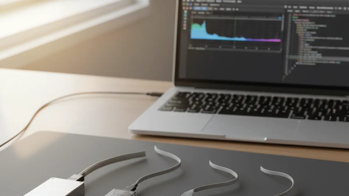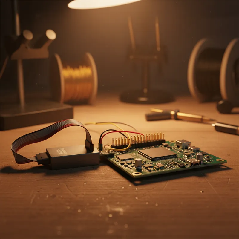
Embedded systems debugging often comes down to one question: “What is actually happening on the bus?” The microcontroller’s SPI peripheral is configured, the code looks correct, the registers are set, but the external device is not responding. Is the clock running? Is the chip select asserted at the right time? Is the data bit order correct? Is the clock polarity what the slave expects?
A logic analyzer answers these questions directly by capturing the actual digital signals on the bus and displaying them in time-correlated waveforms with protocol decoding overlaid. The Digilent Digital Discovery, a USB logic analyzer and pattern generator with 24 high-speed inputs plus 16 digital I/O (40 channels total) and 800 MS/s sampling, provides this capability in a compact, affordable form factor that sits alongside the development laptop.
Why 800 MS/s Matters
Sample rate determines the timing resolution of the captured signals. At 800 MS/s (on up to 8 channels), the Digital Discovery resolves timing events down to 1.25 nanoseconds. At 200 MS/s (on all 24 high-speed inputs), the resolution is 5 nanoseconds.
This timing resolution matters for:
SPI at high clock rates. SPI buses operating at 20-50 MHz require sampling well above the Nyquist rate to resolve setup and hold timing at the edges. At 800 MS/s, a 50 MHz SPI clock is sampled 16 times per period, sufficient to identify timing margin issues.
QSPI flash interfaces. Quad-SPI flash memories operating at 80-100 MHz with four data lines require high-speed capture to verify data eye timing. The Digital Discovery’s 800 MS/s mode captures these interfaces with adequate margin.
Glitch detection. Intermittent timing problems, glitches, runt pulses, bus contention, are only visible with sufficient sampling rate. An 800 MS/s logic analyzer catches sub-5-nanosecond glitches that lower-speed analyzers miss entirely.
Protocol Decoding in WaveForms
The WaveForms software provides built-in protocol decoders that overlay interpreted data on the raw logic waveforms:
SPI. Decodes MOSI/MISO data streams with configurable clock polarity (CPOL), clock phase (CPHA), bit order (MSB/LSB first), and word size. The decoded data appears as hexadecimal values aligned with the corresponding clock cycles, immediately revealing whether the data matches the expected transaction.
I2C. Decodes start/stop conditions, address bytes (with R/W bit), data bytes, and ACK/NACK responses. Identifies which device address is being targeted and whether the slave acknowledged the transaction. For I2C bus debugging, this eliminates the tedious manual process of counting clock edges and interpreting bit patterns.
UART. Decodes asynchronous serial data at configurable baud rates, with parity and stop bit options. Shows transmitted characters in ASCII alongside the raw waveform. Useful for debugging serial console communication, GPS NMEA sentences, and Modbus RTU frames.
CAN. Decodes CAN bus frames including arbitration ID, data length code, data bytes, and CRC. For Indian automotive and industrial teams working with CAN-based systems, this provides bus-level visibility without a dedicated CAN analyzer.
Custom protocols. WaveForms allows definition of custom protocol decoders for proprietary or less common serial interfaces.
Pattern Generator for Stimulus
The Digital Discovery includes a 16-channel pattern generator at up to 100 MS/s output rate. This complements the logic analyzer by providing digital stimulus signals:
- Bus stimulus. Generate SPI, I2C, or UART transactions to exercise a peripheral device under test, useful when the microcontroller firmware is not yet working and you need to verify that the peripheral hardware responds correctly.
- Test patterns. Generate specific bit sequences for production testing, protocol compliance verification, or hardware characterisation.
- Clock generation. Output clock signals at configurable frequencies for clocking external devices during testing.
Practical Debugging Scenarios
FPGA I/O debugging. When a Digilent FPGA board (Arty A7, Basys 3) interfaces with external devices via Pmod connectors, the Digital Discovery monitors the interface signals. FPGA developers use it to verify that their HDL implementation generates correct bus transactions and responds to external inputs as expected.
Mixed-signal debugging. Pair the Digital Discovery (digital channels) with the Analog Discovery 3 (analog channels) for simultaneous analog and digital capture. The shared WaveForms software time-correlates the captures, enabling debugging of mixed-signal systems, ADC conversion timing, DAC output glitches, power supply transient response during bus transactions.
Production test. The Digital Discovery’s scripting interface (Python, JavaScript via WaveForms SDK) enables automated test sequences, generating stimulus patterns, capturing responses, and comparing against expected results. Indian EMS and production test teams use this for low-to-medium-volume production testing where dedicated ATE equipment is not justified.
Why Buy from GSAS
GSAS provides the Digital Discovery, Analog Discovery 3, and the complete Digilent instrument and board portfolio in India with INR invoicing, local stock, and technical support. We serve embedded systems teams across Bengaluru, Hyderabad, Chennai, Pune, Mumbai, Delhi NCR, and Visakhapatnam.
Also appears in:
Interested in Digilent tools?
Talk to our application engineers for personalized tool recommendations.
More from Digilent
View all →
Real-World SDR Applications: 5G Research, Satellites, IoT and ADS-B
28 Aug · 6 min
What Is Software Defined Radio (SDR)? A Practical Explainer for Indian Engineering Teams
19 Aug · 9 min
ZedBoard FPGA-in-the-Loop: HDL Verifier vs HDL Coder
5 Aug · 9 min
AI Data Centers in India: Test, Measurement & Memory Boom
4 Jun · 14 min

Emulating Processor Power for Thermal Testing: Why Constant Power
7 Oct · 7 min

CRPS and Rack Power Supply Testing: The Six Tests That Matter
7 Oct · 7 min