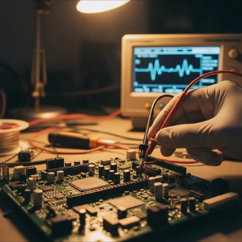
Power Bugs Are Invisible Without Measurement
Firmware power bugs are the most insidious class of embedded software defect. Unlike functional bugs, which cause incorrect behavior that is immediately observable, power bugs cause correct behavior at excessive energy cost. The device works perfectly. Every feature functions as specified. But the battery drains in 6 months instead of 3 years, and the engineering team has no idea why.
The only way to find power bugs is to measure. This tutorial walks through a systematic power profiling workflow using the Joulescope JS220, starting from an unoptimized firmware and progressively identifying and fixing power bugs until the design meets its battery life target.
Setup
Hardware
Connect the Joulescope JS220 in series between the battery (or power supply) and the device under test. The JS220’s banana jack connectors accept standard test leads. Connect the “IN” terminal to the power source positive terminal and the “OUT” terminal to the device’s VCC. Connect the JS220 to the host PC via USB.
For accurate sleep current measurement, ensure that no other current paths exist between the power source and the device, including through the programming cable. Disconnect the debugger (J-Link, ST-Link) during power profiling, or use a debugger that supports power measurement passthrough.
Software
Open the Joulescope UI and verify that the instrument is connected and streaming data. Set the view to the oscilloscope (for waveform analysis) with the statistics widget visible (for real-time mean/max/min current). Set the time scale to show several complete duty cycles of the device.
Step 1: Measure the Baseline
Before any optimization, capture the device’s power profile in its current firmware state. Record:
- Sleep current: The sustained current during the longest sleep period between active events
- Peak current: The maximum instantaneous current during any active event
- Active duration: The total time the device is not in sleep during one complete duty cycle
- Energy per cycle: The total energy consumed during one complete duty cycle (wake through sleep)
Write these numbers down. They are the baseline against which every optimization will be measured.
Step 2: Analyze the Sleep Current
If the sleep current is higher than the MCU datasheet specification for the intended sleep mode, there is a power bug in the sleep configuration. Common causes:
GPIO Misconfiguration
Every GPIO pin that is not configured for its lowest-power state contributes leakage current. The most common offenders:
- Floating inputs: A GPIO configured as a digital input with no external pull-up or pull-down draws current through the input buffer when the pin voltage is in the undefined region between logic low and logic high. Fix: configure unused pins as outputs driven low, or as inputs with internal pull-down enabled.
- Outputs driving into loads: A GPIO configured as output high that drives into a pull-down resistor (or vice versa) creates a DC current path. Fix: set outputs to match their external circuit state during sleep, or disconnect the load.
- Analog inputs left in digital mode: Some MCUs draw more current through a GPIO configured as a digital input than the same pin configured as an analog input (where the digital input buffer is disabled). Fix: configure analog-function pins as analog before entering sleep.
The Joulescope reveals GPIO leakage as a DC offset in the sleep current. After fixing each GPIO issue, remeasure the sleep current. The improvement is immediate and quantifiable.
Peripheral Clocks Not Gated
Many MCUs do not automatically stop all peripheral clocks when entering sleep mode. An SPI peripheral that was used to read a sensor retains its clock if the firmware does not explicitly disable it. A UART configured for receiving keeps its baud rate generator running. Each active peripheral clock consumes microamps.
Fix: before entering sleep, explicitly disable the clocks for all peripherals that are not needed to wake the device. Remeasure with the Joulescope to verify the improvement.
Voltage Regulator Mode
Some MCUs and power management ICs support multiple regulator modes, low-power LDO, normal LDO, and DC-DC switching. The DC-DC mode is more efficient at higher loads but may have higher quiescent current than the low-power LDO mode. If the firmware does not switch to the low-power regulator mode before entering sleep, the regulator’s quiescent current adds microamps to the sleep budget.
Fix: switch to the lowest quiescent current regulator mode before entering sleep. Remeasure.
Step 3: Analyze Active Events
Zoom into a single active event in the Joulescope oscilloscope view. Identify each sub-phase by its current signature:
Oscillator Start-Up
After waking from deep sleep, the MCU’s high-frequency crystal oscillator needs time to stabilize. During this period, the MCU is running from an internal RC oscillator (drawing active current) while waiting for the crystal. If the crystal settling time is excessive (due to crystal characteristics or load capacitor mismatch), this phase wastes energy.
The Joulescope shows the oscillator settling time as the delay between the initial current rise and the start of useful work. If this delay exceeds 1 to 2 ms, investigate the crystal parameters and load capacitors.
Unnecessary Wake Duration
A common power bug is performing operations sequentially that could overlap. Reading a sensor, then processing the data, then transmitting, each as a sequential blocking operation, keeps the MCU active for the sum of all durations. If the sensor read takes 50 ms, the processing takes 5 ms, and the transmission takes 10 ms, the active period is 65 ms.
But if the sensor read can be started with DMA (the ADC samples while the MCU sleeps), and the radio transmission uses DMA for the SPI interface, the MCU active time can be reduced to the processing time plus the setup time, perhaps 10 ms instead of 65 ms.
The Joulescope reveals these optimization opportunities by showing the current profile of each sub-phase with microsecond resolution.
Step 4: Measure the Improvement
After each firmware change, remeasure the complete power profile and update the numbers from Step 1. Track the cumulative improvement:
- Sleep current: baseline vs current
- Energy per cycle: baseline vs current
- Projected battery life: baseline vs current
This before-and-after tracking provides objective evidence that the optimizations are working and quantifies the battery life improvement from each change.
Step 5: Validate
After all optimizations, run a long-duration capture (1 hour or more) to verify that the optimized power profile is stable and that no infrequent events are consuming unexpected energy. Check for periodic current spikes from firmware timers, watchdog services, or background tasks that may not appear in a short measurement window.
Why Buy Joulescope From GSAS
GSAS provides Joulescope instruments with INR invoicing and application support from offices in Bengaluru, Hyderabad, Chennai, Pune, Mumbai, and Delhi NCR. We help firmware teams set up power profiling workflows and interpret measurement results for power optimization.
Contact sales@gsasindia.com or call +91 80 6590 1783.
Also appears in:
Interested in Joulescope tools?
Talk to our application engineers for personalized tool recommendations.
More from Joulescope
View all →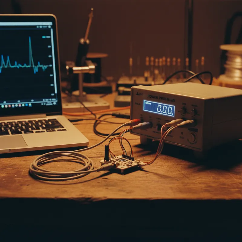
Battery Discharge Profiling for Coin Cell Devices: From CR2032 to 10-Year Life
5 Apr · 7 min
BLE Power Profiling: Measuring Bluetooth Low Energy Current With Joulescope
5 Apr · 7 min
Energy Harvesting and Power Measurement: Designing Self-Powered IoT Devices
5 Apr · 7 min

IoT Battery Life Testing: A Practical Methodology for Indian Product Teams
5 Apr · 7 min

Emulating Processor Power for Thermal Testing: Why Constant Power
7 Oct · 7 min

CRPS and Rack Power Supply Testing: The Six Tests That Matter
7 Oct · 7 min