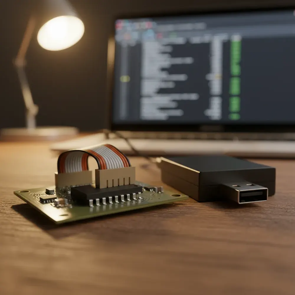
Reading the JEDEC Device ID from an SPI flash chip is the essential first step in any flash programming workflow. It confirms that the Aardvark I2C/SPI Host Adapter can communicate with the flash device, verifies the device manufacturer and part number, and validates the SPI bus configuration (clock polarity, phase, bit rate, and chip select) before attempting to program or read flash contents.
The JEDEC Read ID Command
The Read Identification command is defined by the JEDEC SFDP (Serial Flash Discoverable Parameters) standard and is supported by virtually all SPI NOR flash devices. The command sequence is:
1. Assert chip select (SS active low).
2. Send opcode 0x9F on MOSI.
3. Clock 3 additional bytes while reading MISO, these are the 3-byte Manufacturer and Device ID.
4. De-assert chip select.
For example, a Micron M25P32 responds with 20 20 16 (hex): manufacturer ID 0x20 (Micron/STMicroelectronics), memory type 0x20 (SPI NOR), and memory capacity 0x16 (32 Mbit). A Winbond W25Q32JV responds with EF 40 16: manufacturer 0xEF (Winbond), type 0x40, capacity 0x16 (32 Mbit).
Step-by-Step with Control Center
1. Connect the Hardware
Connect the Aardvark to the SPI flash target using a 10-pin ribbon cable. The pin mapping is:
| Aardvark Pin | Signal | Flash Pin |
|---|---|---|
| 1 | SCK | CLK |
| 3 | MOSI | DI (Data In) |
| 5 | MISO | DO (Data Out) |
| 7 | SS | CS (Chip Select) |
| 9 | GND | GND |
| 10 | VCC (target power) | VCC |
Enable Target Power in the Aardvark menu to supply 3.3V/5V to the flash device if it is not otherwise powered.
2. Configure SPI Settings
In Control Center Serial Software, set the SPI parameters:
- Polarity: Rising/Falling (SPI Mode 0 for most flash devices)
- Phase: Sample/Setup
- Bit Rate: 1 MHz (conservative starting point, increase after communication is verified)
- Bit Order: MSB first
- Slave Select: Active Low
3. Send the Read ID Command
In the SPI Master panel, enter the MOSI data: 9F 00 00 00
The first byte (0x9F) is the Read ID opcode. The three 0x00 bytes are dummy bytes that clock out the 3-byte device ID response on MISO. The Aardvark transmits on MOSI and simultaneously receives on MISO.
4. Read the Response
Control Center displays both the MOSI (transmitted) and MISO (received) data. The MISO bytes corresponding to the three dummy bytes contain the Device ID. The first MISO byte (corresponding to the opcode byte) should be ignored, it is undefined during the command phase.
Verification and Next Steps
If the Device ID matches the expected value for your flash chip, the SPI bus configuration is confirmed correct and you can proceed to flash programming operations (erase, program, verify) using either Control Center, Flash Center Software, or the Aardvark API.
If the response is all 0xFF or all 0x00, check: chip select polarity, SPI mode (try Mode 3 if Mode 0 fails), target power, and physical connections.
Alternative Approaches
The same Read ID operation can be performed through:
- Flash Center Software: automatically reads the device ID during target device selection, with a built-in database of thousands of flash devices.
- Aardvark API: programmatically in C, Python, or C# for automated test scripts that need to verify flash device identity before programming.
- Cheetah SPI Host Adapter or Promira Serial Platform: same command sequence, higher clock speeds available (40+ MHz and 80 MHz respectively).
GSAS Micro Systems provides the Aardvark alongside the I2C/SPI Activity Board and SPI Flash Demo Board for teams learning SPI flash programming workflows across India.
Also appears in:
Interested in Total Phase tools?
Talk to our application engineers for personalized tool recommendations.
More from Total Phase
View all →
Aardvark vs Cheetah vs Promira: Total Phase Host Adapter Guide (India)
17 Jul · 6 min
Automated EV Charger Test Bench in India: GW Instek AC Source, DC Load and Battery Emulator
6 Jun · 16 min
Best Logic Analyzer in India (2026): A Vendor-Neutral Buying Guide for Embedded Teams
5 Jun · 10 min
Capturing I²C/SPI Data to Train Edge AI: A Protocol-Analyzer Workflow for Indian Embedded Teams
4 Jun · 9 min

Emulating Processor Power for Thermal Testing: Why Constant Power
7 Oct · 7 min

CRPS and Rack Power Supply Testing: The Six Tests That Matter
7 Oct · 7 min