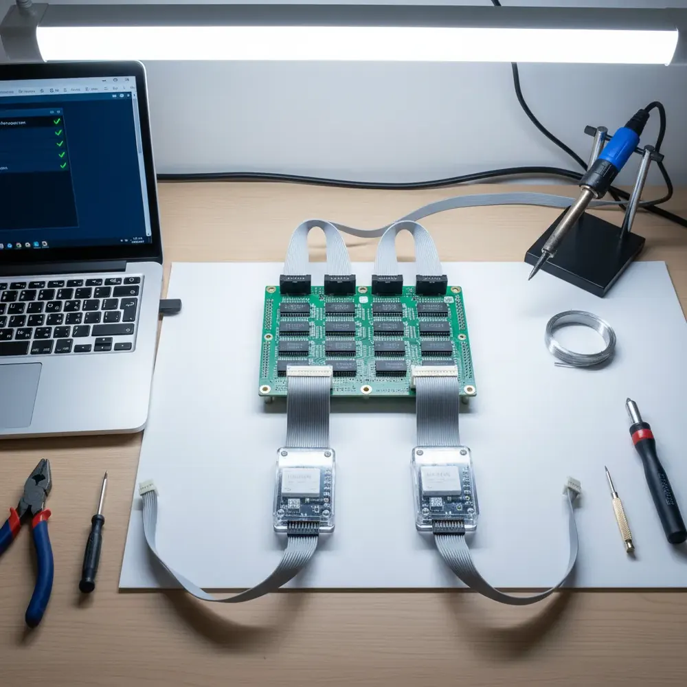
A common production test scenario involves using multiple Aardvark I2C/SPI Host Adapters in a single system to program several I2C chips simultaneously, for example, writing calibration data to multiple EEPROMs on an assembly line fixture. While the Aardvark’s API makes this straightforward from a software perspective, the electrical configuration requires careful attention to grounding and power delivery to avoid intermittent failures and potential hardware damage.
The Problem: Floating Grounds and Insufficient Power
When two or more Aardvark adapters connect to the same target board (or to separate boards sharing a common bus), each adapter’s ground reference may float relative to the others if they are not explicitly tied together. This ground potential difference causes:
- Unpredictable data levels: I2C SDA and SCL signals are referenced to ground, so a floating ground shifts the effective voltage threshold, causing the target device to misinterpret logic levels.
- Flash Center failures: programming operations that appear to complete successfully may actually write corrupted data, or Flash Center may report communication timeouts.
- Interface board damage: if an external level shifter board or interface board sits between the Aardvark and the target, ground potential differences can stress the level-shifting circuitry beyond its rated input range.
The Fix: Common Ground and External Power
Ground rule: All Aardvark adapters and all target devices must share a common ground reference. The Aardvark provides two ground pins on its 10-pin header specifically to ensure a solid ground path. Connect all adapter ground pins to a common ground bus on your test fixture. Power rule: When using an interface board or level shifter between the Aardvark and target devices, disable the Aardvark’s target power output on all adapters and supply 3.3V from an external bench power supply. The Aardvark’s target power pin can supply up to 25 mA at 5V, sufficient for a single EEPROM but not for powering interface boards with multiple level-shifting channels. Overloading this output risks damage to both the Aardvark and the interface board.
Step-by-Step Configuration
1. Wire all ground pins from every Aardvark adapter to a common ground bus on the fixture. Use short, low-impedance connections.
2. Disable target power on every Aardvark adapter (in Flash Center: uncheck “Enable Target Power” in the adapter settings; in API: do not enable target power in the configuration call).
3. Supply external 3.3V from a bench power supply to the interface board’s VCC rail.
4. Verify ground continuity with a multimeter before powering on, ensure less than 0.1 ohm between all adapter ground pins and the target board ground.
5. Test with a single adapter first before adding the second and subsequent adapters to isolate any per-channel issues.
Applies to SPI Too
The same grounding and power rules apply when using multiple Aardvark adapters for SPI communication. SPI signals (MOSI, MISO, SCLK, SS) are equally sensitive to ground reference differences, and the higher SPI clock rates (up to 8 MHz) make the system even more susceptible to noise caused by ground loops.
GSAS Support
GSAS Micro Systems provides applications engineering support for multi-adapter test fixture design, including guidance on grounding schemes, power distribution, and API integration for parallel programming workflows. Contact your local GSAS FAE for fixture design consultation.
Also appears in:
Interested in Total Phase tools?
Talk to our application engineers for personalized tool recommendations.
More from Total Phase
View all →
Aardvark vs Cheetah vs Promira: Total Phase Host Adapter Guide (India)
17 Jul · 6 min
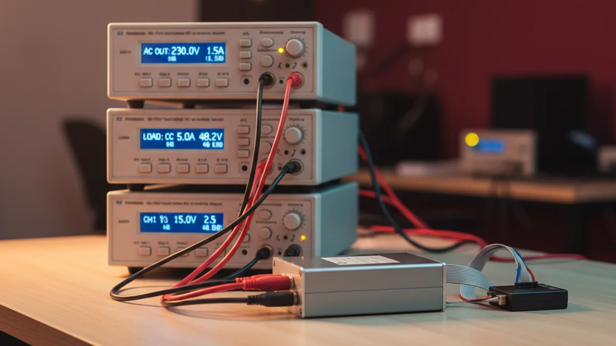
Automated EV Charger Test Bench in India: GW Instek AC Source, DC Load and Battery Emulator
6 Jun · 16 min
Best Logic Analyzer in India (2026): A Vendor-Neutral Buying Guide for Embedded Teams
5 Jun · 10 min

Capturing I²C/SPI Data to Train Edge AI: A Protocol-Analyzer Workflow for Indian Embedded Teams
4 Jun · 9 min

Emulating Processor Power for Thermal Testing: Why Constant Power
7 Oct · 7 min

CRPS and Rack Power Supply Testing: The Six Tests That Matter
7 Oct · 7 min