The Lab Programmer’s Role
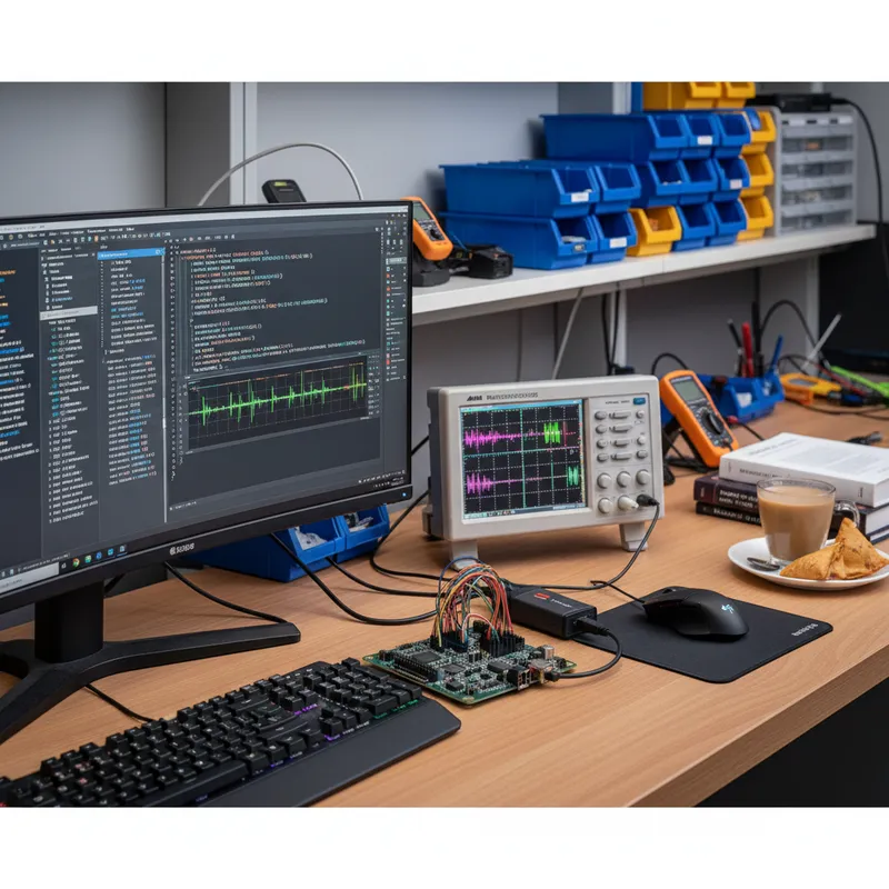
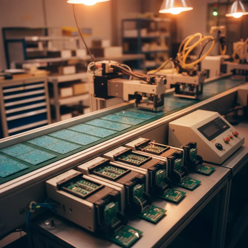
In every electronics product’s lifecycle, there is a stage between firmware development (where engineers use debuggers and evaluation kits) and production programming (where inline systems program thousands of boards per day). This intermediate stage, firmware recipe validation, NPI first-article programming, small-batch sample builds, and engineering lab support, needs a dedicated tool that bridges development flexibility with production-grade traceability.
The ProMik MSP2100Net fills this role. It is a compact tabletop ISP programmer designed for firmware developers, NPI engineers, and R&D teams who need multi-protocol programming capability with FlashTask Pro project management.
Hardware Architecture
The MSP2100Net provides 16 independently configurable I/O channels that support multiple programming protocols without external adapter boards:
| Feature | Specification |
|---|---|
| Form Factor | Compact tabletop / desktop |
| I/O Channels | 16 independently configurable |
| Protocols | JTAG, SWD, SPI, UART, I2C, CAN |
| Network | 100/1000BASE-T Ethernet |
| USB | USB 2.0 host port |
| Power Supply | Integrated programmable target power |
| Software | FlashTask Pro with project management |
| Traceability | Serial number logging, pass/fail tracking |
The 16 I/O channels are configurable per-pin, meaning the MSP2100Net adapts to different target device pinouts through software configuration rather than hardware changes. A firmware developer working with a Cortex-M MCU today and an SPI flash device tomorrow uses the same programmer, reconfigured in FlashTask Pro.
Ethernet Connectivity
Unlike USB-only lab programmers that require a physical connection to a development PC, the MSP2100Net connects via Gigabit Ethernet. This enables:
- Remote operation: programme target devices from a different room, floor, or building. Useful for environmental test chambers, EMC labs, or secure areas where physical access is limited.
- Network integration: the MSP2100Net appears on the factory or lab network, accessible from any workstation running FlashTask Pro
- pOnline Pro management: integrate the lab programmer into the centralised programming management infrastructure alongside production systems
Programmable Target Power
The integrated programmable target power supply simplifies bench setups. During development, the target board may not have its own power supply assembled or available. The MSP2100Net provides configurable voltage and current to the target through the programming fixture, eliminating the need for an external bench supply.
Development Workflow
Firmware Recipe Creation
The firmware developer creates a FlashTask project on the MSP2100Net:
- Import the firmware binary (HEX, S-Record, binary, ELF)
- Configure the target device (MCU family, protocol, clock speed, voltage)
- Define the programming sequence (erase → program → verify → configure option bytes → lock)
- Run the sequence on a development board and verify correct programming
- Iterate on the recipe (adjust erase sectors, add security configuration, tune clock speed for optimal throughput)
The validated FlashTask project file is the deliverable from this process, a portable, self-contained programming recipe ready for NPI and production.
NPI First-Article Programming
When the first production PCBs arrive from the contract manufacturer, the NPI team uses the MSP2100Net (or the XTL-m manual station) to programme first-article samples. The FlashTask project from development runs unchanged. The NPI team validates:
- Correct firmware version programmes successfully
- Verify operations pass (read-back matches source)
- Programming test points on the PCB make reliable contact with the fixture probes
- Cycle time meets production planning requirements
- Traceability logging captures all required data
Handoff to Production
The validated FlashTask project transfers directly to production systems, XTL-s, XTL-i, or rack-mounted XDM-USB/XDM-ETH, without modification. This zero re-porting capability is the MSP2100Net’s key contribution to the production workflow: it ensures that what was validated in the lab is exactly what runs on the production floor.
Multi-Project Lab Support
R&D teams often work on multiple products simultaneously. A lab in Bengaluru or Hyderabad may have engineers working on an automotive ECU project (Cortex-M7, JTAG), an IoT sensor (Cortex-M0+, SWD), and a communication module (SPI flash), all needing programming support.
The MSP2100Net’s multi-protocol support and software-configurable I/O channels handle all three projects from a single instrument. FlashTask Pro stores separate projects for each product, and switching between projects takes seconds, select the project, connect the target, programme.
This consolidation reduces lab equipment costs and bench space requirements compared to maintaining separate single-protocol programmers for each project.
Comparison with Development Debuggers
Engineers sometimes ask why they cannot use their existing JTAG debugger or SWD probe for production programming. The key differences:
| Capability | Development Debugger | MSP2100Net |
|---|---|---|
| Programming speed | Moderate (debug-optimised) | Optimised for throughput |
| Multi-channel | Usually single | 16 configurable channels |
| Project management | None (bare binary upload) | FlashTask Pro with version control |
| Traceability | None | Serial logging, pass/fail tracking |
| Production portability | None (different tool for production) | FlashTask projects transfer to XTL/XDM |
| Verify operations | Basic (checksum) | Full read-back comparison |
| Target power | External supply needed | Integrated programmable supply |
The MSP2100Net is not a replacement for the development debugger, engineers still need debuggers for stepping through code, setting breakpoints, and inspecting memory. But for the programming task itself, loading firmware into a device reliably, repeatedly, and traceably, the MSP2100Net is the appropriate tool from NPI onward.
Applications in Indian R&D Labs
- Automotive R&D in Pune and Bengaluru: ECU firmware development and validation programming
- IoT product development in Hyderabad and Bengaluru: multi-protocol programming across diverse MCU families
- University and research labs: flexible multi-protocol programming for academic research projects
- NPI teams at EMS providers in Chennai and Noida: first-article programming and process validation
Why Buy from GSAS
GSAS Micro Systems is the authorised ProMik engineering partner in India, providing the MSP2100Net with INR invoicing, FlashTask Pro licensing, and programming workflow consultation. Engineering teams in Bengaluru, Hyderabad, Chennai, Pune, Mumbai, Delhi NCR, and Visakhapatnam support firmware developers and NPI teams with device configuration, project setup, and production handoff planning.
Explore the MSP2100Net and ProMik product range, or contact us for evaluation and pricing.
Also appears in:
Interested in ProMik tools?
Talk to our application engineers for personalized tool recommendations.
More from ProMik
View all →
Automotive ECU Programming and Traceability: Meeting IATF 16949 with ProMik
5 Apr · 7 min

Scaling Electronics Manufacturing in India: Programming Infrastructure for Growth
5 Apr · 7 min
FlashTask Pro: Production Programming Project Management with ProMik
5 Apr · 7 min
Gang Programmer vs Inline ISP: Choosing the Right Production Programming Approach
5 Apr · 7 min

Emulating Processor Power for Thermal Testing: Why Constant Power
7 Oct · 7 min

CRPS and Rack Power Supply Testing: The Six Tests That Matter
7 Oct · 7 min